Hello everyone,
I am quiete new to this forum, although I made a prototype project with SimpleFOC and the G431 ESC Kit. My plan is as follows:
I am building a 4 wheeled robot with another fifth motor for other purpose (regular DC motor). I plan to use four BLDC motors from Nanotec like this one: DF45M024053-A2 - Bürstenloser DC-Flachmotor | Nanotec , which is only equipped with Hall Sensors.
I bought a BLDC driver and was able to achieve a minimal rotational speed of ~60 rpm, which is low enough, although less would be better. I tested the same motor with the mentioned B-G431B-ESC1 and was able to get better results on low rpm, but on higher rpms some kind of jittering occurred.
Nevertheless i am very happy with the results so far.
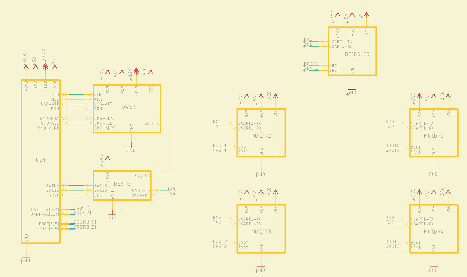
So my next step would be to design a custom 5 in 1 ESC PCB (logic very simmilar to this one:)
based on the G431 MCU with Power delivery and connector for other boards.
I have made some own, basic pcbs in EAGLE, but want to switch to KiCAD for this project.
Unfortunately I do not have more experience with STM32 ICs other than the B-G431B-ESC1 kit, so I wanted to ask, how a roadmap for this project could look like and on what things I should have an eye on. Are there any reference designs in KiCAD for a project similar to this one?
Any help? Also, I can answer any questions if more info is needed.
Usually it’s the other way around, halls give good high speed performance but stutter at low speed. If you’re printing any debug output, turn it off. STM32’s serial implementation is problematic that if you make two calls to Serial.print within a few milliseconds of eachother, the second one will block processing and cause the motor to stutter. A single call can print a fairly large amount of data without blocking, but even two single-character prints in a row will block it.
You can try SmoothingSensor to improve low speed. Just create SmoothingSensor smooth(hall, motor); and motor->linkSensor(&smooth); and it will do its thing. You can also call motor->linkSensor(&hall); while running to compare the performance with and without smoothing.
My Gooser is not KiCAD, but still good to learn from, or use it directly since it’s basically what you want. Some of the GPIO pins can be used to control a separate DC motor driver, or if you have an ESP32 or something for wireless communication then it could handle the DC motor.
The Smoothing is actually a good idea, I will definitely have a look into that!
I am not sure about the correct state of my PID tuning (if it is good enough for both low and high speeds).
I have to design my own solution somehow, because my application needs a different form factor, but the reference design is a good starting point.
Could you maybe also share, how you started and what is important for debugging pcbs other than obvious details?
@Valentine created a simple design called Lepton (sadly no longer available, and impossible to manufacture anyway since the SE3082G mosfets no longer have the internal drain-source connection, and there are no substitutes), and I reworked it to be even simpler without a buck converter for my 12V powered robotic bird wing project where I need high power and small size/weight.
That got me accustomed to the essential components of BLDC drivers and the general process of PCB design (which to me feels like the ultimate puzzle game, trying to get all the signals where they need to go in minimal space by clever placement of each component and which MCU pins to use for which purpose). After burning two of them, I decided current sensors are also an essential component.
Then I watched a bunch of Robert Feranec videos on youtube and gained the ability to “see” electric fields when designing. High frequency energy (anything digital) travels in the dielectric rather than copper conductor, and if the outgoing and return conductors move apart from eachother, the field blooms outward to bridge the gap and will induce/be induced by any other fields in the same space. 4-layer PCBs with solid ground planes on the inner layers are like a cheat solution to the problem since the return current can travel directly underneath the outgoing line, 0.2mm away where the field remains very compact. But when a signal via goes between top and bottom layers, you also need a ground via nearby for the return current to travel to the other inner layer (“return current” is a misleading name, BTW. Both currents travel outward from the source together and meet up at the other end).
For debugging, my toolkit is a multimeter, oscilloscope, and cheap USB microscope (great for finding solder problems). I’d hold off on buying the oscilloscope until you encounter a problem you can’t solve without it. Make some small probes for use with the multimeter and oscilloscope. Solder pieces of ~0.8mm copper wire onto each end of a flexible silicone wire and sand one end to a slightly-blunted sharp point. Nickel plating would be nice; I have to to lightly sand the tip before use to remove oxide. The other end can be alligator clipped to the multimeter or hooked by the oscilloscope probe.