Lepton Deku mod

Continuing from here https://community.simplefoc.com/t/lepton-v2-revised-design-tested-working-30v-80a-mosfets/2489/43

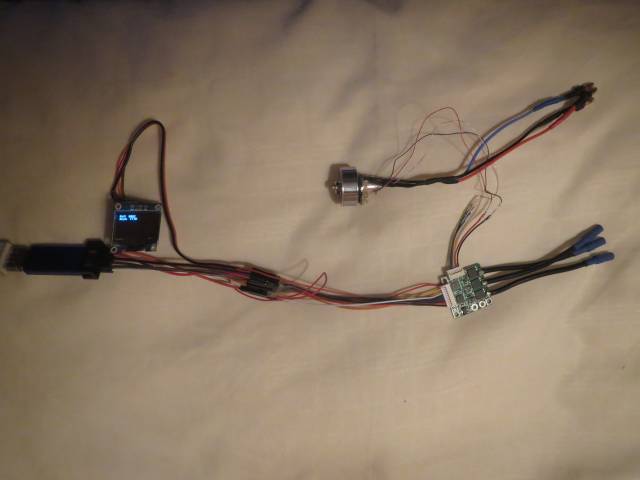
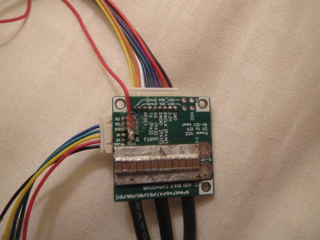
My boards have arrived, and they are ever so lovely. Unfortunately I don’t have the 9 pin female cables to connect to them with, so I can’t actually test just yet unless I want to try soldering wires to the 1.25mm pitch pins on the underside (I might).

I do have 6 pin cables though, and can confirm that both the XKB connectors and HCTL are compatible with cheap cables off ebay.

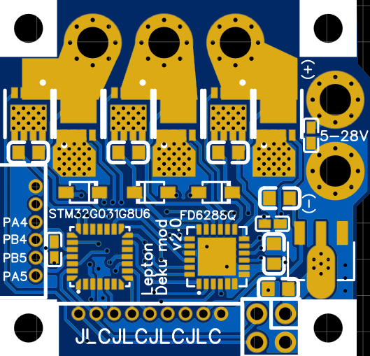
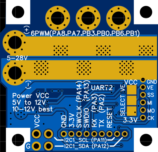
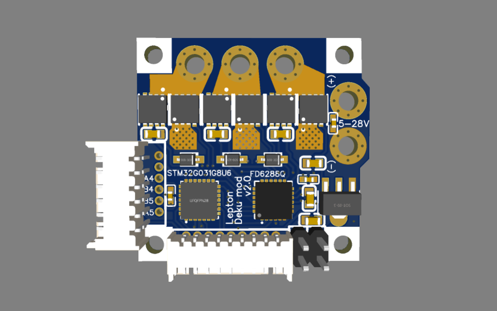
Here is what the front and back look like as they come from JLCPCB.


Then to boost the current capacity, take a piece of 2mm copper wire and hammer it out to about 3x1mm rectangular.
Hammer

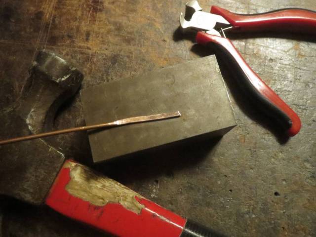
Clip off a couple pieces, bend them as flat as possible, and then sand to perfection. I used my trusty extra-extra-coarse DMT Dia-sharp stone.
Flatten

Then tin them with solder while holding with pliers, apply some flux to the board, and stick the copper bars as well as 12 ceramic capacitors in place (now you can see why I put the JLC order number where I did :slight_smile:). Getting the first copper bar tacked down was a bit tricky because it wants to slide around in the flux and/or molten solder. Once that’s done, you can use tweezers to push the other bar and capacitors up against it while soldering. Add more solder on the capacitors, and then reheat the first bar to make sure it’s fully seated.

I was worried the transistors would fall off the front while I was soldering these large pieces on the back, but it seems my fears were unfounded. It’s easy to tell when the solder under the copper bar melts, so you can stop before the heat has time to soak through and hit melting temperature on the other side.

On the front side, I added some blobs of solder to help conduct current from the S2 pin of each transistor to the vias that go through to the ground rail. I touched the capacitor on the far right with the soldering iron and it got sucked into the blob, so I had to re-solder it in its original location. No harm done.

So there it is, exactly as I had envisioned! Why isn’t this the standard method of constructing motor drivers? 4 layer PCBs and 2oz+ copper are so expensive, yet here you can have even heavier conductors with just a little bit of manual soldering. I’m already having visions of doing it with these monster TOLL-8 MOSFETs and playing this on loudspeakers in the back yard while I test it https://www.youtube.com/watch?v=ERKnkHq-6XA

Heck, you could even load pre-made copper bars on a pick-and-place machine and solder them with paste like any other SMD component. Better still, use finned heatsinks as the conductors :grin:

Thank you again to Valentine for providing the basic layout and component selection, and answers to my many questions :slight_smile: Such a liberating feeling to add PCB design to my skillset.

4 Likes

That’s pretty awesome.

Any microelectronics project involving a big hammer and a blowtorch is definitely worth doing!

Most welcome. That’s the main reason why we are all here.

Cheers,
Valentine

Im interested to see how much current this board can handle now, very cool design!

Turns out being unable to test was a good thing, because I noticed a flaw in my plans that could have fried the MCU! I was going to power the digital hall sensors using the mid-voltage rail because they need more than 3.3V, but that would only work with exactly 5V (the minimum the gate driver can use, and maximum the I/O pins can tolerate). I have a 5V regulator that I can use for now, but I’ll see if can find some latching hall sensors that run on 3.3V to eliminate the need for the voltage selector entirely. Any recommendations? This is what I currently use https://www.sparkfun.com/products/9312

Same here :slight_smile: The MOSFETs are rated for 80A continuous 170A peak, but with 5mOhm on-resistance, 80A would be 32W dissipation, which is the equivalent of a soldering iron. 40A/8W dissipation seems like a more reasonable continuous current to shoot for. Still a lot to get through that itty bitty S2 pin and the vias, but I don’t see how 2oz or 4 layer could provide any significant improvement there. I really only need about 20A, but getting 40A in 1 square inch for less than $6 per board would be good for my ego :stuck_out_tongue:

I’m not entirely sure what you say here, but you are aware that the Hall effect sensors are open-collector type. So pulling them op to the MCU power does not fry anything, even if they are powered with 12v

Regarding the gate voltage; you can possibly reach better performance with lower rds(on), if you switch with eg. 10v, but that creates a whole avalanche of design considerations. I’m betting on 10amp!

Higher is better because the MOSFETs need 10V to fully open (5mOhm, versus 7.5mOhm at 4.5V)

Was just looking at the board, and it does look like you can power the gates with 12? If you just pull up your halls to MCU voltage, then you’re good to go.

Maybe observe the LDO temperature if you intend on 12v for switching power.

Oh! Thanks for not assuming that I know what I’m doing :laughing: I was thinking they would either output the voltage of the VCC or GND pin depending on north or south magnet detected. But yes, the pullup resistor in the application circuit does imply that it either outputs GND or nothing. I always just used the internal pullups on ATmega8, although they are higher value than the recommended 10k. STM32 is about the same, ~40k internal pullups. Hopefully that’s ok.

And yes, my plan was always to power the gates with 3 cell lipo, 11.1V nominal. Although I would like something less fire-prone for testing. Maybe I’ll try a 12V ATX power supply, or a car battery (that could certainly explode the MOSFETs, but probably not itself).

But before even that, I just need to get something uploaded to the STM32. I think I can use the 3.3V from the ST Link and leave the gate driver and LDO unpowered for that. I’ve got STM32CubeProgrammer installed, and Arduino IDE able to compile SimpleFOC for “Generic G031K8Ux” (G031K8 is listed in the same group as G031G8 in the datasheet), so I think I’m all set. I cannot use SimpleFOC Commander due to 64KB flash size, but that’s ok. Without it I have 11KB free, and I don’t need anything fancy for communication.

You may have challenges with the internal pullups, maybe not. Just reminding you that the Doc recommends external resistors. 3.3k is somewhat stronger pullup then 40k…

Thats not a certain fact. Some programmers need to know the on board MCU voltage in order to burn the HEX file. Im not familiar with the ST Link. The ST Link 3.3v could be a probe, ensuring that the MCU is powered correctly.

You got this! Burn it

The ST-Link has a “Target Voltage” input, that isn’t intended to power the project. It receives the target MCU voltage, but doesn’t provide voltage.
Nonetheless, some of my clone ST-Link V2 provide 3.3V here, but the official ones don’t.

Success so far! I found a folder called G031G(4-6-8)U_G041G(6-8)U in the Arduino stm32 library. It was only missing its entry in boards.txt, and the .ld file in the folder itself which could just be copy/pasted from another since it really only specifies the ROM/RAM base addresses. So now I’m for sure compiling for the right MCU. Surprisingly the serial pins in variant_generic.h are already set correctly for the UART2 that I’m using.

The ST Link V2 ebay clone worked without issue, and does indeed provide both 3.3V and 5V power. Driver installed automatically when connected, and STM32CubeProgrammer was able to operate it and uploaded a simple program that calls Serial.println once per second. Then I switched to FTDI adapter for serial communication, and the text does indeed appear in Arduino IDE’s serial monitor! I can’t believe it all worked on the first try.

Next task is to get my little OLED display hooked up so I have output without having to switch back and forth between ST Link and FTDI for every upload. With that I can try powering the hall sensors using the ST Link’s 5V and see if manually turning the motor changes the angle reported by the HallSensor class as it should. Then comes the nerve wracking part, actually powering the motor :slight_smile:

2 Likes

Yes, this is definitely a good thing. Glad it worked out.

After a great deal of head banging I finally got the OLED display to work. In the end the main problems were that I had the wrong I2C address (my old code had it shifted up one bit for convenience when writing directly to the ATmega TWI registers), and the silkscreen on my Lepton is wrong. SDA and SCL are PB7 and PB8, not PA11 and PA12. Those were for I2C2 in an earlier revision. Though upon further consideration I would like to put it back that way, with the I2C2 pins on the programming connector and I2C1 on the two solder pads for communication. For one thing it may be difficult to get I2C1 to act as both master for the OLED and slave for whatever is sending out motor target position commands. And for another, separate buses will make it easy for each Lepton to have its own OLED even when several are connected together on the same I2C1 lines for communication. Better for debugging complex robots.

So now I can view the hall sensor output while manually rotating the motor, and while I do get some response, it’s not quite right. Could be sensor placement, the weak pullups, or something else. Will continue investigating.

HallTest

Some good news is that the SE3082G MOSFETs have been restocked, so this is not just a one-off design. Although I had been toying with an alternate version using 6 single-channel 3x3mm MOSFETs. These in particular are attractive for their 1.2mOhm on-resistance. The board size is unchanged aside from a 1mm protrusion for the power input terminals. Unfortunately the heavy conductors must be closer together, so there’s no space for ceramic capacitors between them anymore. But it is back to having 4 mounting screw holes, and holes for the motor wires. Ideally you would solder some bits of copper about 5x2x1mm between the MOSFET pins and motor terminals, but solder blobs would be better than nothing. It would also be possible to machine small blocks of copper with two m2 threaded holes in them (crossed but not intersecting), so you could screw the blocks to the board and use lugs on the motor wires. Solder is probably better at this size, but when scaled up for larger MOSFETs that may be a good design.


1 Like

That’s very educational thank you.

You need to be careful scaling up for larger mosfets because this driver cannot drive anything more than a few hundred mA gates. You will either burn the driver with large mosfets of be forced to put large gate resistors and the mosfets will operate inefficiently.

Either way that’s really nice. Post more pics of the LCD screen setup, please.

Cheers,
Valentine

I currently have a wire soldered onto the Lepton’s encoder voltage selector (with a bit of hot glue for strain relief), which provides 5V power from the ST Link to the hall sensors (and incidentally the LDO and gate driver).
CablesBack

The 9 pin cable goes to a 5x2 pin header (with more hot glue). Two pins are jumped together for GND, and two for 3.3V. Next is SWDIO (purple) and SWCLK (brown), then TX (green) and RX (blue), and finally SDA (yellow) and SCL (orange). I didn’t have any larger 2-row headers on hand, so I just soldered a single pin to reset (white). Same for the 5V line.
CableConnector

I would have soldered female Dupont connectors directly to the 9 pin cable rather than using the header pins, but unfortunately it turns out my cheap jumper wires are copper-plated aluminum and don’t solder worth a darn :stuck_out_tongue:

The ST Link has dots of paint on it to remind me which wires to plug where when switching back and forth with the FTDI earlier on :slight_smile:
STLink

The hall sensors on the motor each have two 0603 capacitors soldered between their leads, and 3-filament litz wire to connect to the cable. The red litz goes to the VCC of each sensor, and has the filaments joined together at the other end. Black goes to the GND of each sensor and similarly joined, and the uncolored one goes to each of the output pins of the sensors. Much easier to keep track of than if you solder the 3 filaments of one litz to the 3 leads of one hall sensor. Then you have to check continuity at the other end to sort out which filament goes to which pin. This way only the signal wires would have to be checked to see which filament goes to which sensor, but since that doesn’t matter anyway you don’t have to check anything :grin:
MotorCloseup

Let me know if there are any specific points you want more focus on.

1 Like

Looks like my problem is sensor placement. I tried a different motor and it steps through the hall sequence and tracks the angle properly as I turn it. It has the sensors farther out from the center, so I think I just went a little too far inward on this one in my desire to keep the sensor leads from protruding past the rim. Oh well, only a few grams of aluminum wasted.

Yeah, I assumed the gate driver would need to be scaled up too, although I don’t understand how to read the datasheets on them. Comparing this FD6288 with the IR2136 from your Krakatoa, the max power dissipation is about the same, and IR2136’s Output short circuit pulsed current ratings are significantly lower. I don’t see any other values that seem related to power output.

Comparing the MOSFETs, I’m guessing the total gate charge is what determines how much current it takes to turn them on. 51nC for Lepton’s, versus 165nC for Krakatoa’s, so a little over 3x as much. Or for medium size, something like this with 128nC (~2.5x Lepton’s).

So to charge and discharge that each PWM cycle, 25kHz * 51nC * 2 is 2.55mA. And since a BLDC driver has 6 of them that’s 15.3mA total. By the same math for Krakatoa’s 165nC you get 49.5mA. That seems reasonable in relation to IR2136’s 200mA Output high short circuit pulsed current, but FD6288’s 1.5A seems like maybe this isn’t the right parameter to be looking at. And if you say FD6288 can handle a few hundred mA, then maybe I’m not doing the gate charge math right either…

Just found a neat math trick on YouTube while researching gate-resistors.

Take your 165nC divide it by the time in nS (nanoSecund) and you get the current needed through the resistor.

So 165nC/200nS =0,825 amp. (14,54ohm resistor)

This does not mean your resistor will dissipate all that heat since the heat dissipation will be averaged over time.

Thanks! Is the 200nS an average of the MOSFET on/off switching time? The one with 165nC gate charge has 44.9nS turn-on delay and 116.6nS rise time, so 161.5nS total, and then 102.7+112.5=215.2nS total for turn-off. And how did you get from 0.825 Amp to 14.54 Ohm?

And Lepton’s MOSFETs have much shorter switching time, and no gate resistors at all. How can the little driver survive that but not survive the larger MOSFETs with resistors?

The time is determined by the current that can flow into the gate. That also determines the switching time. The times given in the datasheet are samples, given for certain test conditions/assumptions. Your actual times depend on the gate resistances you choose.

The 200nS was just a example and the resistor is based on 12v switching voltage. Better use equation provided by @runger

Another thing to consider is the gate trace inductance or ringing/noice in the gate trace. That is mainly why I’m looking at the gate resistor. In this TI app note they use a 7 ohm resistor to dampen the noice on a MOSFET with 118nC total gate charge.

Very useful graphic! However neither of the gate driver datasheets lists internal resistance. The Lepton MOSFET datasheet doesn’t list gate resistance either, but others of similar power seem to be 1-1.5 Ohm. So with 12V that’s around 10A. But the listed 20nS turn-on delay + 15nS rise time implies 1.5A gate current. Or does current only flow during the rise? That would be 51nC/15nS=3.4A. In any case it’s a lot more than a few hundred mA unless the gate driver provides a lot of resistance and slows down the switching time. And the Krakatoa MOSFETs have lower current when calculated that way, 165nC/162nS=1A with turn-on delay+rise time, or 1.4A with rise time alone. Of course higher average as calculated previously, but still not even 50mA for all 6 of them. So I’m still not clear on how you calculate what a given driver can deal with.