Good point, I think it will be paramount to have mixed decay code for optimal stepper control. The goal is to minimize the ripple current and the winding_heating, but coding it will be a challenge. Definitely a plus to control the deadtime between phase_direction change.
With fast decay, negative voltage is applied to the winding by switching on the opposite FETs and reversing the direction of current flow through the H-bridge. Fast decay enables the motor to respond quickly to changing step inputs, but it results in a slow stop of the motor. The downside of fast decay is that it causes high current ripple.
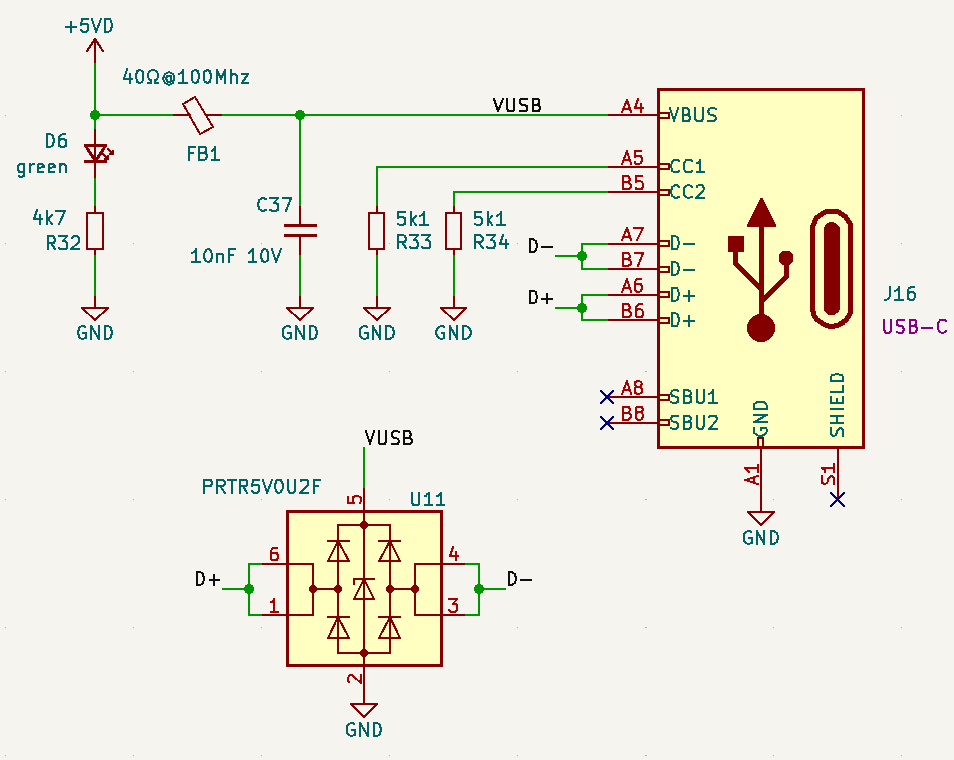
Yes, I’m going for the 2.0 type. Good to know they kept the 2.0 standard for the C type.. The micro B connectors is sometimes rather flimsy. I’m thinking C type is much better for machine use although the cables are a tad expensive. The USB lines are broken out to solder the wires to the board, so if people want a minimalist version that could work.
I would just make everything USB C these days, to future-proof it. As you probably know USB-C will be mandated soon by EU law for a bunch of devices classes, and I believe this means it will gradually replace micro USB for everything over the next years.
And I agree they are far more robust, have a better “feeling” when using them, and also more convenient due to the double-sided thing.
With USB-PD, which doesn’t look too complicated really, then you can even get 6A@20V over the USB lines, which could be enough for some motor applications… that would mean power and fast comms in one shielded and convenient cable. Now we just need some multi-port USB-PD hubs capable of 120W on each port that’s a product class that’s still missing as far as I’m aware
Hmm tempting project to make a USB-PD hub, but I don’t mind running 12v vires on the machine if I can save the PD wires cost. I actually think most people, when building a CNC machine, will prefer to solder in the com lines, but of course that is preferences.
note: I know the STM32H747 is out of stock @the moment, just looking.
The STM32H747 has three dedicated SPI ports. It is quite funny how, the physical footprint is very similar to a single core MCU. Breaking out two of the SPI ports will make it possible to communicate with the AS5247U, although im not exactly sure if the dual SPI interface it supported, yet. The only downside, is that the ENCODER interface will have to be interrupt_based and not hardware Encoder_interface, which is on the advanced timer. TIM1/TIM8. Unless I wire the sencond SPI to the breakout_header and run the hardware ENCODER pins on TIM8 to the SMD_underside header pins connected to the regular sensor interface. That way, one can still connect a dual SPI interface, but will need to solder jumper wires to the sensor, breakout, or implement a SPI interface on the TIM8/ENCODER pins.
Edit: Maybe Im mistaken…
TIM2, TIM3, TIM4, TIM5 all have independent DMA request generation. They are
capable of handling quadrature (incremental) encoder signals and the digital outputs
from 1 to 4 hall-effect sensors.
The timer, when configured in Encoder Interface mode provides information on the sensor’s
current position. Dynamic information can be obtained (speed, acceleration, deceleration)
by measuring the period between two encoder events using a second timer configured in
capture mode. The output of the encoder which indicates the mechanical zero can be used
for this purpose. Depending on the time between two events, the counter can also be read
at regular times. This can be done by latching the counter value into a third input capture
register if available (then the capture signal must be periodic and can be generated by
another timer). when available, it is also possible to read its value through a DMA request.
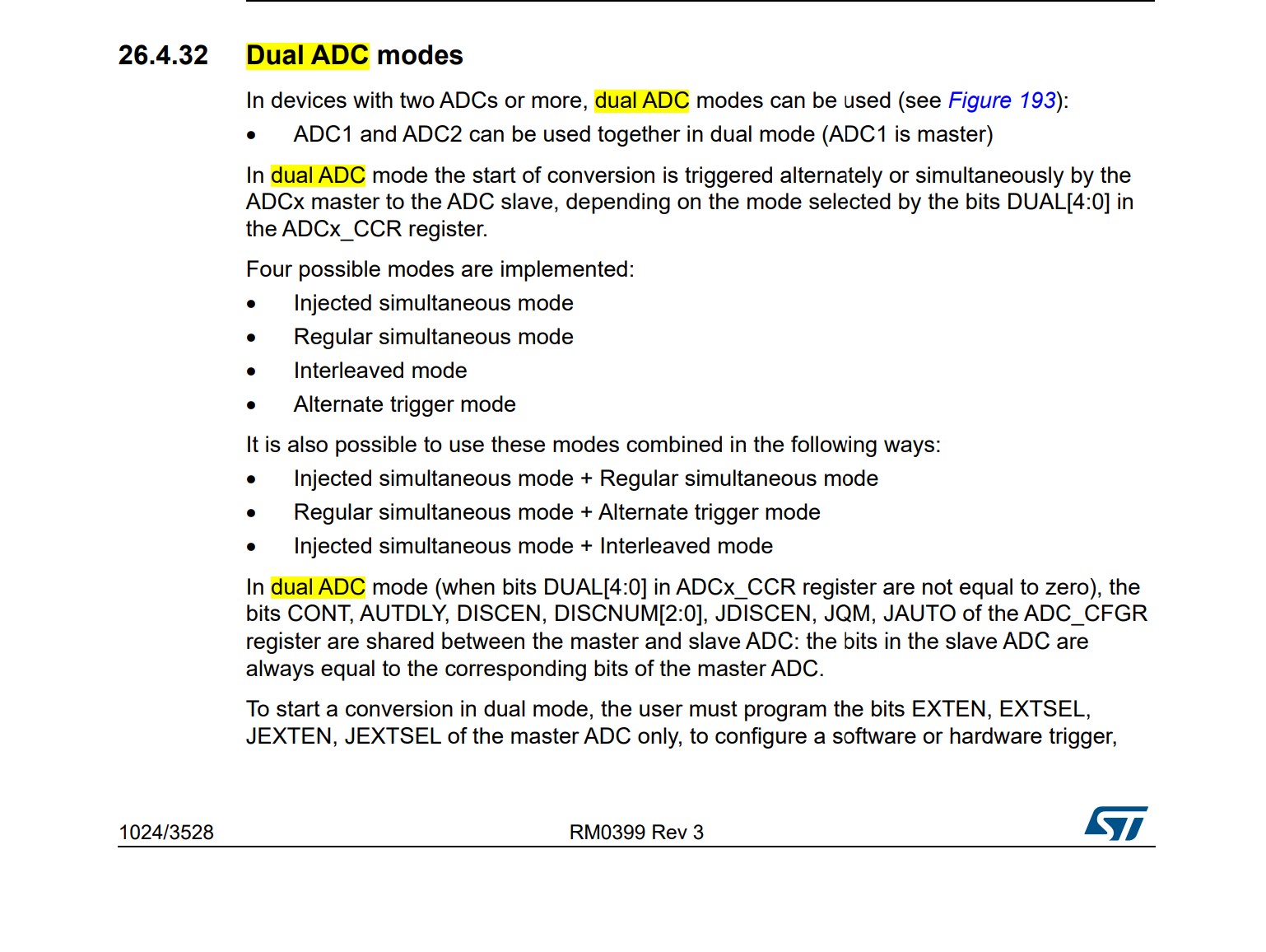
The two current sense ANALOG input are assigned to ADC12_INP4 and ADC1_INP2, which should make it possible to use the dual ADC mode, for simultaneous samples.
That leaves ANALOG temperature (thermistor) port and ANALOG voltage_divider (BUS voltage) port on ADC3.
The HALL and ENCODER interface is on TIM3 CHA 1-3
All BLDC PWM signals are on TIM1 (Advanced Timer). Supports 4PWM stepper and 6PWM BLDC.
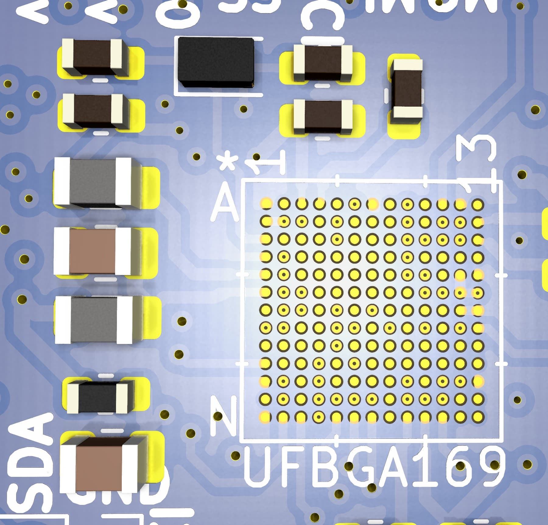
Luckily the boards are only 20mm x 42mm, but I agree in that prototypes will be more expensive, since the fab house can´t pool the design. In bulk production, prices will drop exponentially. Of course the same can be said about the MCU itself. Regarding the price, the real question is, if it can compete, as a use_case specific alternative to the Portenta H7 Light.
For prototypes, I believe I will have to reflow the boards myself. I do have a reflow oven, so if it works with just a bit of flux, I think it could be done. The datasheet does not specify anything about stencil opening recommendations for this package.
Its a 4 layer design. Even though the MCU footprint itself is tricky, the routing actually becomes cleaner, since I connect directly to VIA_IN_PAD.
Knowing the reflow_temperature profile for those chips will make it easier to do.
@runger Do you think an external memory through QSPI is necessary. If so, then I think it could work with 6 layers. Perhaps the pins are taken, haven’t checked. Maybe a small SMD SD card? Priority is TIM1 and TIM3 for ENCODER/HALLs. Apparently the TIM3 can work in a synchronized way with TIM1 doing the FET switching.
We could do a Crowd campaign, but that would require SimpleFOC support and proof of concept, so prototypes are kinda needed.
I’m really surprised you can fit it on 4 layers - with 13x13 balls I’d expect at least 6 layers and blind vias. And even that probably won’t even let you access all the pins… I think normally chips like this need HDI designs and maybe stacked vias, but TBH I can’t find much good material on how to lay these out. If you have any pointers they’d be very appreciated!
Yes, well, blind_vias is another process on top of the micro_via laser mowing. If the vias are laser_burned through the stackup, I think they are less troublesome to fab. Or do you think they shoot each layer w. thou laser, before they are stacked. From what I gather, the 0.1mm laser hole, does not need filling, since the plating is enough to close the gap.
Edit: I think I can fit a onboard SD card in there, but it does require some re_routing. Is it really needed for motor control purposes. The great thing about an external SD card, is that the USB could boot up a folder on the PC/MAC, for programming the MCU by dragging a file and resetting. Another way is to just flash the devise through USB?
Another argument is the possibility to have a INIT document in the SD card, which can be changed and saved by the user w. stuff like, basic settings or routines.
I think once you want things like that you have to talk to your fab.
I can tell you for example, that PCBWay, whom I like to work with, wouldn’t do laser vias in any kind of normal process. It was only available for the PCBA HDI design process, which is a lot more expensive.
And I think the laser vias are just for relatively short depths, I don’t think you can just laser a 0.1mm hole in a 1.6mm PCB, but I could be wrong. But even if you can, the aspect ratio will be so tall, it will be hard to plate such a via, and it will be very fragile…
In a “normal” PCB you won’t get laser vias, and if you want blind vias, each level-pair will be its own drilling and plating run, and so add significantly to the cost.
And you can only place vias between layers that satisfy certain properties. E.g. you can go from layer 1 to layer 2, or from layer 1 to layer 4, or from 3 to 4, but not from 1 to 3, or from 2 to 4.
So I think to route out all the pins would need like a 12-layer PCB with 5 blind via runs - at that point I think you can just make it a HDI design, and it will even cost less.
But of course if you only need a “sparse” routing, where most of the pins don’t get used, you might have enough space to get traces in to all the pins you do need on even just 4 layers, or even using through holes…
If using stacked uVia’s, a thin PCB thickness is preferred.
The only way to sketch it up in kiCad is to align several microvías (blind/buried vías) pointing to the right layers. The only way to achieve different size anular ring between outer and inner layers. It may not be possible in KiCad. That may require a expansion, or plug-in. Edit: Just found out, that choosing Blind/burried vias in KiCad, lets you place them stacked. So various size annular ring between layers in a uVia stack is possible in KiCaD.
Edit: @runger You are right about the HDI perspective. I guess it is a mindset of sorts, if blind vias from layer one L1 to layer two L2 is possible, then routing below that via is suddenly possible and it opens up some new pathways.