Gooser: a 4-in-1 Lepton derivative

Finally placed the JLC order after making a bunch more edits.

  • Changed net names on each copy of the 14mm section so I can run DRC on the 8-motor version without getting a ton of errors.
  • Discovered that at some point early on I moved the left side pin header down by 0.1mm but forgot to move the right side one to match, so the holes were slightly off when copy-pasted, putting them too close to some traces and vias.
  • Added thermal reliefs on the connector ground pins. I don’t like setting the copper area to spoke mode because I do want the capacitors to have maximum conductivity even if they are a little tougher to solder, but there’s no need to suffer on the connectors. To solve it, I temporarily change the pad net names when rebuilding the copper areas to leave a clear space around them, and added traces to cross the gap.
  • Added a voltage divider on the back for the main bus voltage. It’s not connected to anything, but can be wired over to the ADC12_IN10 pad to allow voltage monitoring.
  • Copied input area onto the right side of the board, so when cutting them in half I’ll get two full-featured ones. This involved removing the extra pin header from the right side to avoid pinching the input rail width, but I had no particular plan to use it anyway.
  • Extended motor wire pads by 2mm, similar to how I did on past versions. They’re easy to sand off if desired, or can be cut off before manufacturing by moving the board outline. This allows using two 14mm long capacitors per motor and bending them down to lay over the mosfets. Previously there was just barely enough room, but would have been difficult to get the tip of the soldering iron on the pad without touching the capacitor.
  • A few minor grounding improvements.
  • Added timer/current sense information to the silkscreen.

I got a stencil this time, after finding that you can specify a size smaller than the full sheet, and if <200x200mm, the added shipping cost was only $4. Though the stencil itself was still rather pricey at $14 with the recommended electropolishing option for 0.5mm pitch.

Now I just have to make up my mind what all components to buy and how many motors worth…


1 Like

The boards have arrived! I only have enough mosfets for one motor right now, but that’s all I need for testing. I’ll order a bunch if I can ever make up my mind which ones to buy.

Anybody have an opinion whether I should use 30V or 40V mosfets with 24V power supply? The difference in resistance is about double, but still half that of my old friend SE3082G. 1.2mOhm for the 30V JMSL0302AU-13, 1.7mOhm for 30V BSZ0901NS (same ones used on Antun’s DriveShield), and 2.7mOhm for 40V AGM403AP.

I think the SMM4F26A TVS diode from ESC1 can only protect the 40V ones since it breaks down at 28.5-31.5V, and is still not 100% safe with 42V clamping voltage. But I think ESC1 has 35V ceramic capacitors, so maybe that’s ok? The next lower SMM4F24A looks like it would provide some protection for 30V mosfets while still being (I think) safe to use at 24V supply voltage, but would need 40V mosfets for full safety with 39V clamping voltage. And still not fully safe unless I use 50V capacitors, which I’d rather not since they’re huge. 35V can fit two 470uF per motor bent down over the mosfets, whereas 50V would need one big one per motor on the back side of the board to avoid blocking either the connectors or motor wire pads. Maybe 50V ceramics and 35V electrolytics would be safe enough? On the theory that the ceramics will charge up quickly, but the electrolytics will suppress typical transients before charging above 35V. But maybe something like a hoverboard motor could still kill them.

I’d also appreciate any opinions on the JMSL vs. BSZ0901 for <18V applications. JMSL is marginally better in terms of resistance and price, but Infineon is a more well known brand and it feels like a waste not to buy them while they’re on sale. Maybe I’ll just get some of each.


2 Likes

Assembly complete! CPU is programmed and running, so I will proceed with testing the drivers next.

First I cut the board into a dual and quad. In the process I learned why JLC says no copper in the V-cut area… broke the tip off my only V-bit trying to cut .5mm deep all at once, and after regrinding it and taking .1mm passes there was a terrible burr of copper I had to chisel off before the board would lay flat to cut another groove from the other side. I’ll try a downcut mill next time.

Making the copper bars was moderately difficult. Started with 2mm wire, hammered flat, annealed, bent the corners, hammered flat again, annealed again, refined the bend, filed the inner corners sharper, and then sanded flat on coarse diamond stone. Technically it only needs to be flat on one side, but it looks nicer without the oxide coating from annealing. Accidentally cut the bottom side copper bar a bit shorter than intended, but no big deal.

My notecard with rolled masking tape to hold tiny capacitors is still serving me well.

I didn’t use the stencil since most of my components are pulled from GooserCS and SimpleFOC Stepstick and have solder on them already, so the stencil would give too much.

I had more trouble than usual with components blowing away from the heat gun, but eventually got them all wrestled into place. Also got my first tombstone. 0402 capacitor stood right up. But no problem to shove it back down with tweezers.


You may notice there’s solder on the back side M1 mosfet pads… that’s because I soldered them over there first, and had to pluck them off and reinstall in the correct location. I also forgot the VDRV snubber. I tried to solder it on with the iron, but failed due to heatsinking of the ground pad (on a related note, the thermal relief on the programming connector ground pad was wonderfully effective). But it’s non-essential, so I’ll leave it off for now and add it along with the mosfets for the other motor later.

Soldering the copper bars was a challenge for the heat gun. The second one came out ok since I pressed it down firmly before heating, but the first one had a gap under it because I could only melt portions of it at a time, so it never self-leveled. I eventually managed to get it down by combination of hot air blower and soldering gun. But for the 8-motor board, I will definitely need an oven.

At first I thought I’d go the traditional toaster oven route, but after a bit of research people seem to struggle with insulating them well enough, so I think I’d be better off building a smaller enclosure from scratch. Aside from that it’s just a heating element, temperature sensor, solid state relay, and arduino to control it.

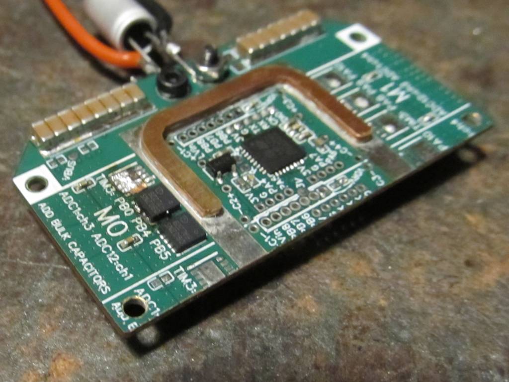
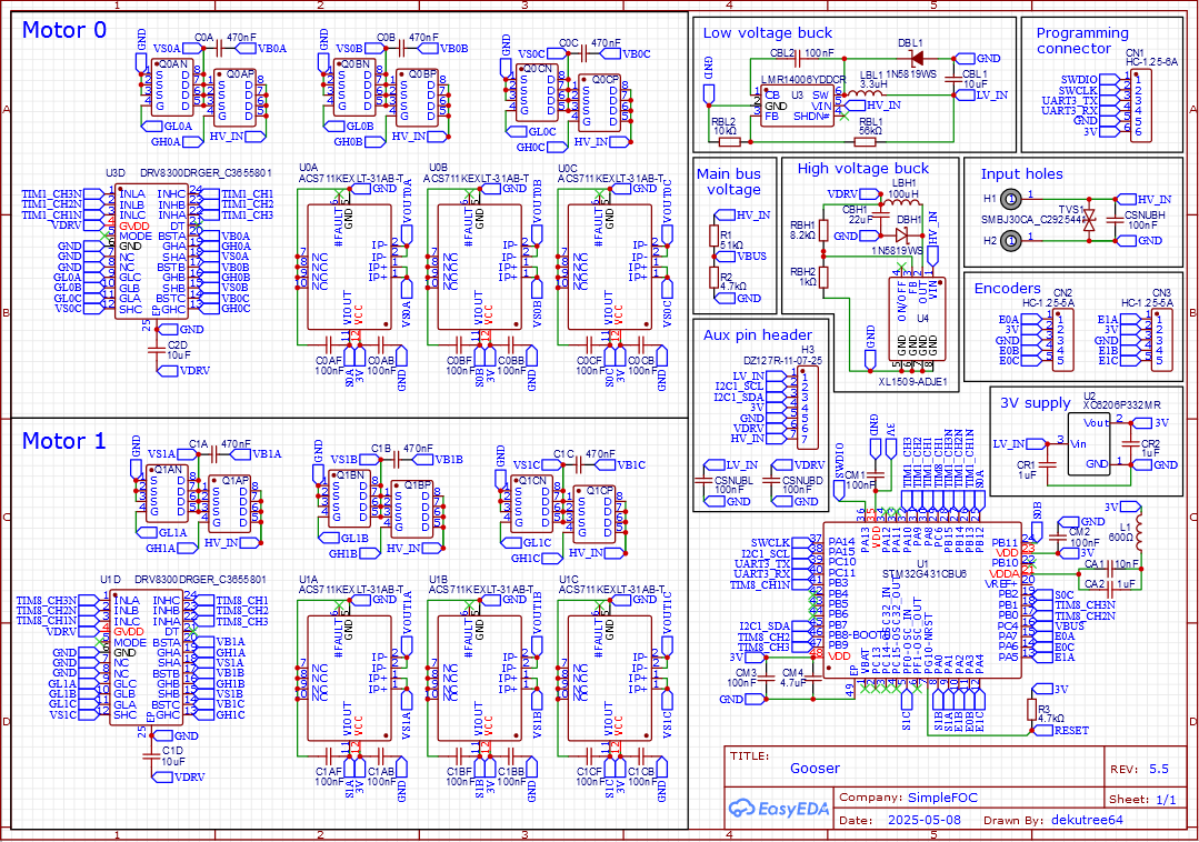
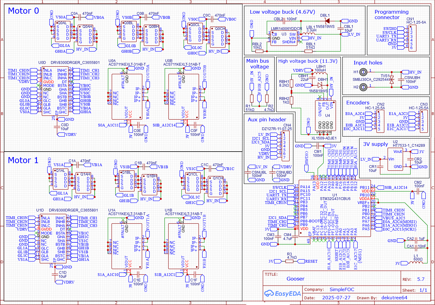
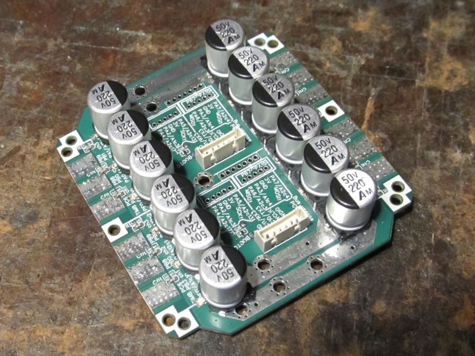
Failure. Phase A mosfets burnt instantly upon connecting the battery. No visible damage to the package, but a small orange flame and plenty of smoke, and solder obviously melted since some squeezed out from under one of them. 0 resistance on all their pins, so power to ground, outputs, and gates are all shorted together.

Thankfully my standard procedure is to plug and unplug quickly, and if nothing bad happened then plug it in and wait to see. So no further damage during the half a second or so of burning aside from the capacitor also losing a leg. It may have still been alive, but they’re cheap enough I just tossed it and soldered on a new one.

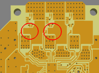
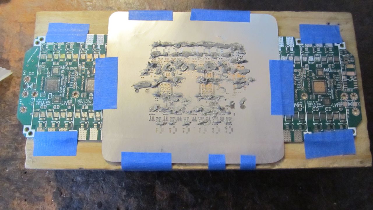
I removed the burnt mosfets, though they had apparently welded themselves to the PCB copper and wouldn’t come off without a bit of pulling, which peeled the copper up from the fiberglass.

The remaining mosfets seemed to be ok, so to verify that it was not just a solder short or other undetected anomaly, I plugged it in again (even more briefly this time) and got the same result on phase B. Smoke and solder squeezed out from under one of them. No flame though, and the capacitor was only slightly warm so I think it’s ok.

No idea what the problem is yet.


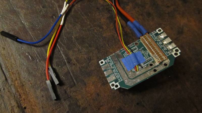
UPDATE: Removed all mosfets so I could probe the drivers without anything blowing up. Only low side B was welded to the PCB copper this time, but high side B is also internally shorted. Two good mosfets left for further testing.

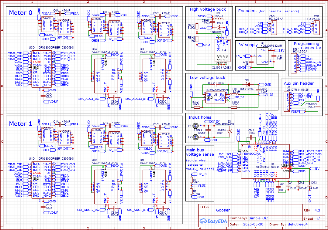
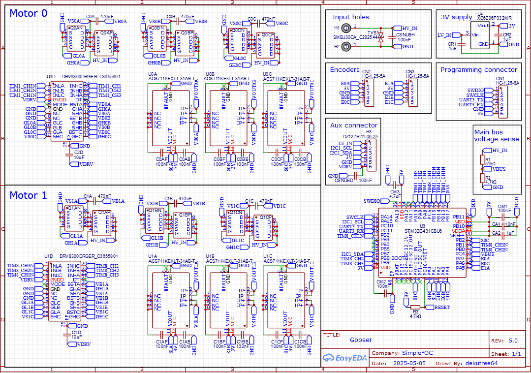
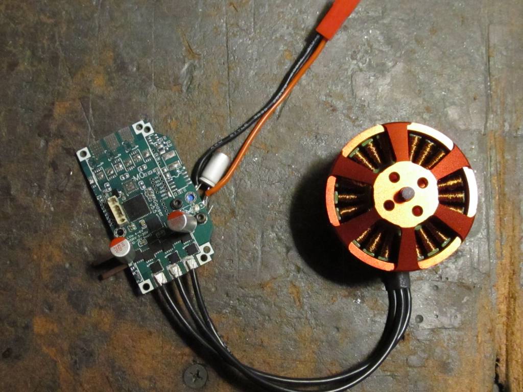
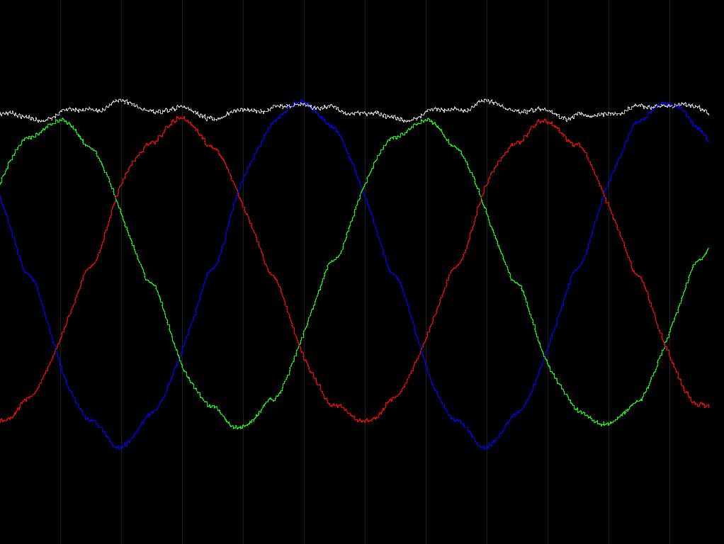
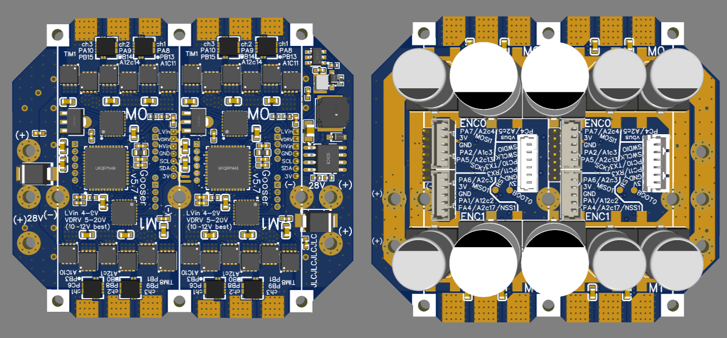
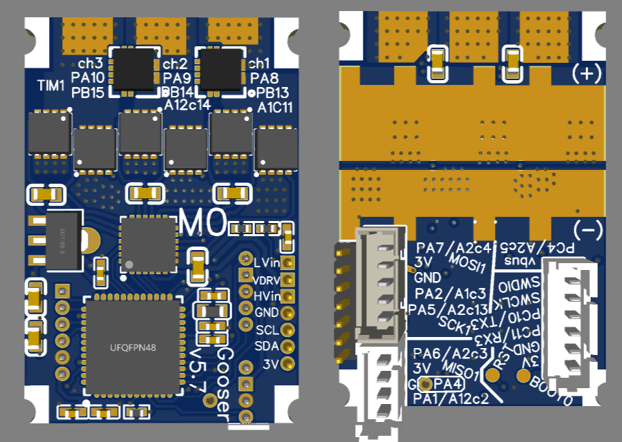
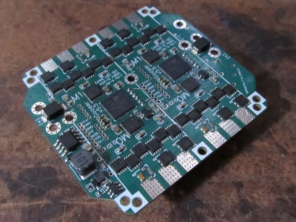
The drivers are receiving proper PWM inputs and outputting inverted waveform on the low side, so that confirms it is properly configured for 3PWM. High side gates are all flat at 5.7V (running on 7.4V lipo). Unsure if that was just due to having the mosfets disconnected, I reinstalled the phase C high side mosfet, and it remains the same. So it seems the high sides are on enough to conduct (though not properly boosted by the bootstrap), and whenever the low sides switch on via PWM it short circuits and dies.

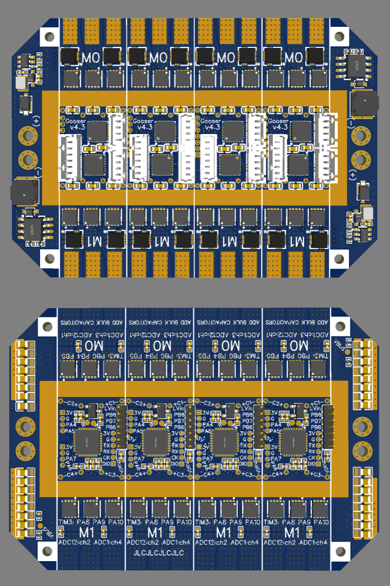
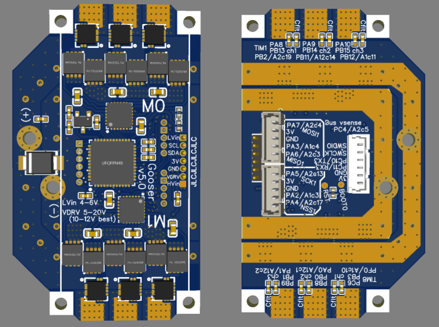
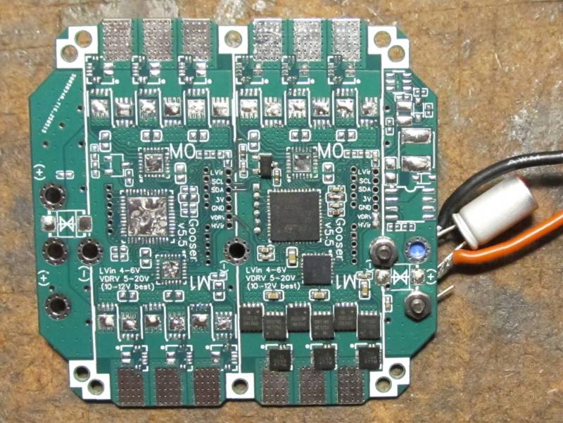
The M1 driver inputs and outputs are all the same, so it seems unlikely to be a bad driver or soldering problem. I’ve double checked that the wiring is identical to GooserCS (which is still working fine with mosfets transplanted from Lepton). Not sure what to try next.

UPDATE 2:
Confirmed on Gooser3 that DRV8300 should output boosted high side PWM even without mosfets. The only difference there is that it’s configured for 6PWM, but since the low side signals are the inverted ones, I doubt that would change the high side behavior.

Swapped out the M0 driver on Gooser4 with a different one since I couldn’t think of anything else to try, and no change.

This is maddening.

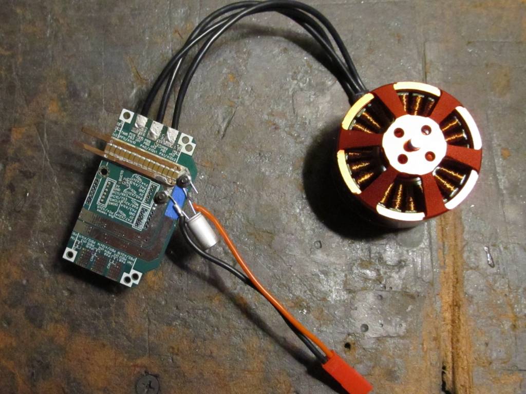
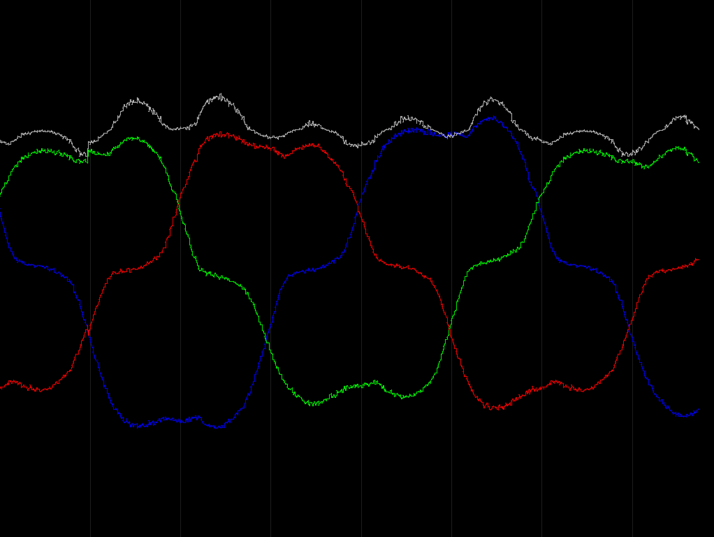
UPDATE 3: I installed the driver I removed from Gooser4 onto Gooser3 (still without mosfets) to verify it would behave the same as the other, and it does not. The inputs are all being driven properly by the CPU, but the low side outputs are chaotic, mostly 0V but frequent blips up to 6-7V with no regular period. Phase A high side is flat 6.2V. Phase B high side is about the same but slightly ripply. Phase C high side has blips like the low sides, but with the floor slightly above ground. The blips also show up on the BSTC pin, but in that case the floor is the 7.4V battery voltage.

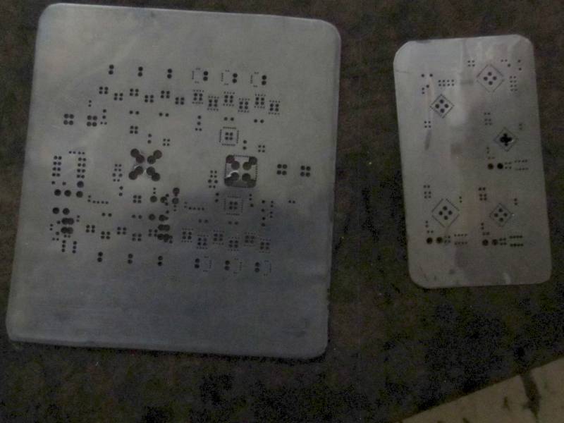
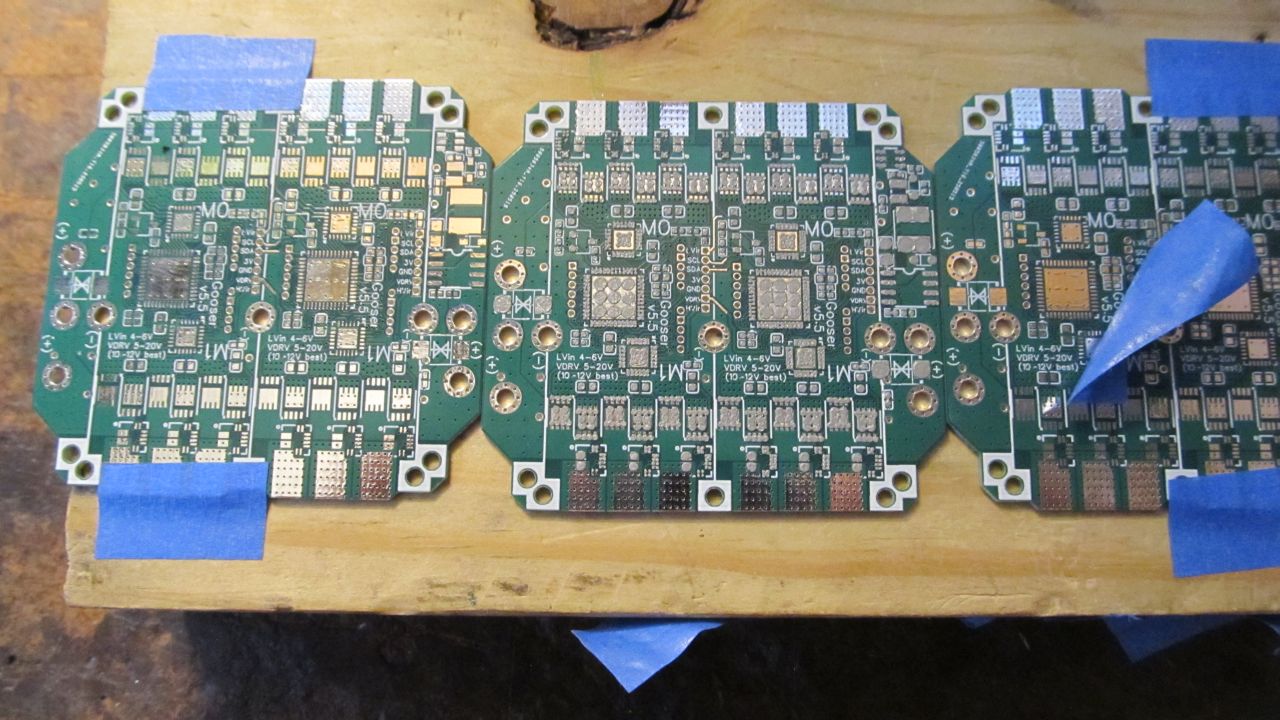
I wish I had some new DRV8300’s to test with. The ones I’ve been using were pulled from GooserCS with the heat gun so they shouldn’t be heat damaged, but these unpredictable results indicate otherwise. I’ve been painstakingly checking for solder shorts between every pair of pins and every pin and ground, so I’m fairly certain that hasn’t been a problem. It’s possible the ceramic capacitors have been heat damaged after so many reflow cycles, but I don’t know any way to test that except for replacing them with new ones, and again I only have others pulled from GooserCS.

I’ll buy one complete set of components from Mouser and start fresh.

UPDATE 4:
Nope. Removed both drivers and their their capacitors, and the one mosfet I still had on the board. Installed the brand new driver and capacitors in the M1 slot, and the old mosfet to see if it would make any difference compared to the other phases. Same behavior as before. High side outputs always on but not boosted, and low side outputs giving proper inverted PWM.

I am 100% stumped. If anyone can help, I would be forever grateful. Otherwise it’s back to the drawing board again, and hope I don’t step on whatever landmine I stepped on this time.

The drawing board it is, then!
Gooser5 - Platform for creating and sharing projects - OSHWLab

At least I’m getting faster. Two days and I think this one is ready to ship. Routing was very much easier this time due to having 50% more space.

This version is based on Gooser3 so I’m back to 6PWM and 3-channel current sense and stacking two 4-motor boards on top of eachother. And thanks to the single mosfets taking more horizontal space and less vertical, I was able to get the CPU on the top layer so JLC can do all the difficult assembly.

No buck converters this time, but I’ll probably make a version with them later.


UPDATE:
Had the idea to see if I could fit the larger 3V regulator from Lepton, and I can if I move its capacitors to the back side. But it’s only rated for 100mA despite its higher 500mW thermal rating, which is right on the line of being enough, and 500mW is not enough to allow joining it with a 10V driver supply anyway, so I’ll stick with the little one.

The only thing that really bothers me about this design is these pinch points in the VS areas:


If I go down to 2 channel current sense, I could eliminate the leftmost sensor and shift the middle one left to clear up more space. But will the increase in conductor area outweigh the loss in efficiency from lower current sense accuracy?

UPDATE 2:
And here is what it looks like. Undecided which to go with. Another option would be to move the mounting holes outside the white lines so the top left and bottom right sensors can be moved over. That would make the minimum-width version of the board less user-friendly, but might be worth it.

As usual, I’ve gone totally overboard optimizing this thing. I went to place the order yesterday, but apparently JLC’s US shipping network has gone down in the trade war and I’ll have to pay $23 for UPS, so I decided I’d better add the buck converters now rather than validating the basic design first. That led down a long series of revisions, ultimately resulting in the left-side input area becoming somewhat superfluous.

My original intent was to have power input on the left and bucks in the upper right, above where you would cut off for single-motor. But it seemed like a waste not to add some input holes in the otherwise empty lower right. However the aux header encroaches on the ground path, and the path to M0 on the top layer is entirely blocked by the bucks, so maximum battery current will be limited when using these input holes (I think high motor current at low RPM will still be ok, only circulating in the mosfet areas). So I left the original input area too, and added two more options for positive input.

To solve the mounting hole conundrum from before, I did move them outside the white lines, but also added a second set of mounting holes on the white lines but spaced 50mm in the y direction. My robot needs the original 46mm spacing, but this provides an elegant solution for minimum-width boards too.

I’ve also positioned the ground input holes where they can serve as mounting holes when cut to single-motor size. I moved the programming connector out of the way as best I could, but the corner slightly overlaps the ground hole pad when soldered on the top side of the board.

Amusingly, the central area turned out to be tileable after all. The 3V regulator and SDA/SCL pins are on the opposite side of the board from the aux header, so those lines had to get most of the way across anyway. That just left VDRV, and it was able to get through the sparse lower left area with little difficulty.

I added a ferrite bead for the analog supply, after seeing it in the B-G431B-ESC1 datasheet.

The last thing I need to do before ordering is to try a stencil making technique I saw on youtube. It would be great if I can avoid wasting money on stencils for failed designs or shipping after validating. But it’s not that much wasted money, so if it’s too much trouble making them myself I’ll order it.


1 Like