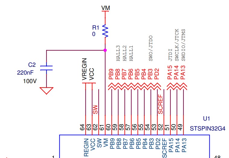
Do you have a opinion on the 0R resistors in the STM reference design. Eg. on VM line ?
Does it act like a kind of choke or what´s the deal with those ?
It’s a routing trick to (pick one):
On reset the SWD pins are internally pulled up.
![]()
I don’t think you need to add anything to the SWD lines on STM32 - you could check some of their reference designs with SWD headers, but I can’t find anything so far. Of course you could add some ESD protection or other protections if you wanted to make the board super-professional and tough to break but it all costs money and takes space…
On the VM line it’s a bit confusing. I think the intention is to cut the VM from the STSPIN when you’re not using its buck converter. The there is probably another way to to supply VCC.
It’s just like a solder bridge… remove it to disconnect that signal. They have them in various places in this schematic for example to disconnect the ST-Link.
OK so it’s a “no-mount” solder bridge. Good to know.
I agree, if the pins are just SWD, then they have their internal pull-up/down in order. It’s only because I’m using the SWCLK line as HI on the 4th bridge driver, I want to make sure it does not bounce around and accidentally trigger the High side FET.
If it floats for just a short while during the transition from reset to setup there might be some weird undesirable behavior of the driver.
I made room for two 0402 to tie that 4th driver low, when not in use, as recommended by the driver dataset.
Another component question;
Why does STM use 0805 caps for the boot circuit (1uF / 25V) when the same value is easily found in 0603 package ?
Does the boot caps develop heat, which makes the larger package better for heat dissipation…
This is the one in their BOM
https://www.digikey.dk/en/products/detail/würth-elektronik/885012207078/5453527
Found this pretty good explanation for future refence:
It is probably important to mention that the reduction of capacitance with increasing voltage is not a property of all capacitors. It only really applies to ferroelectric dielectrics like barium titanate, used in X5R and X7R types. These are the most common surface mount capacitors, due to their small size for the capacitance. Other common dielectrics do not suffer from this effect. Polyester film, polypropylene film, mica and NP0 types have almost constant capacitance regardless of voltage applied. Also, polarised electrolytic types don’t change with voltage either
I guess the 0805 caps are prioritized due to prize vs size consideration compared to NP0 caps (1uF/25V).
Hmm… NP0 is not an option in that range = 1uF - 25v @Mouser
Now we´re at this topic of CAPs. Do you see any reason not to add capacitance to the VM input. The reference design use a single 200nF (0.2uF/100V), but looking at mouser it is possible to find 1uF/100V/X7R in 0805 package. So why not use one of those, maybe also a 0.47 uF and the 0.2 uF?
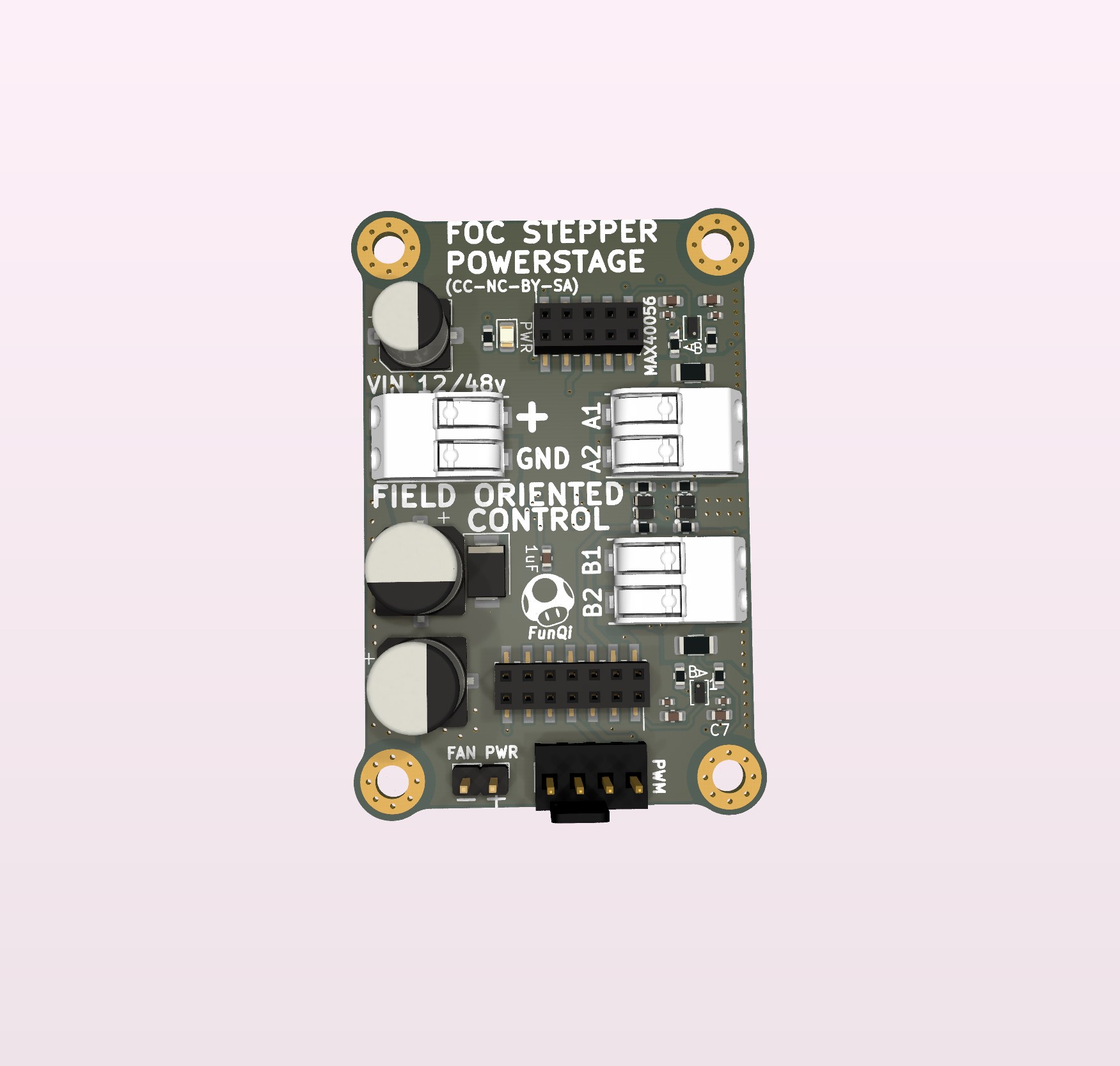
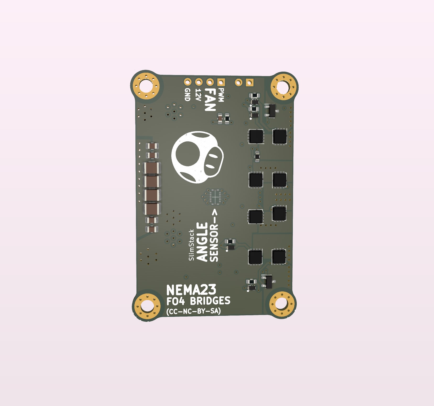
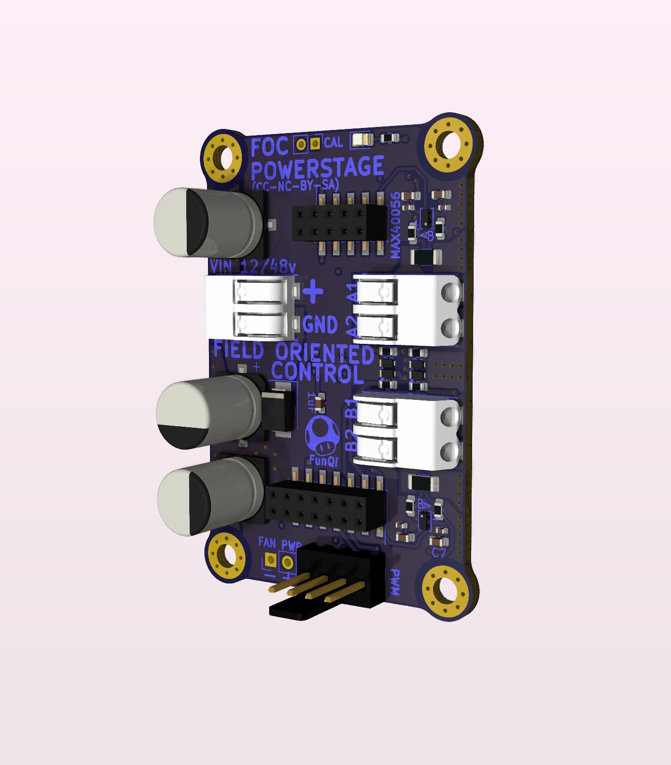
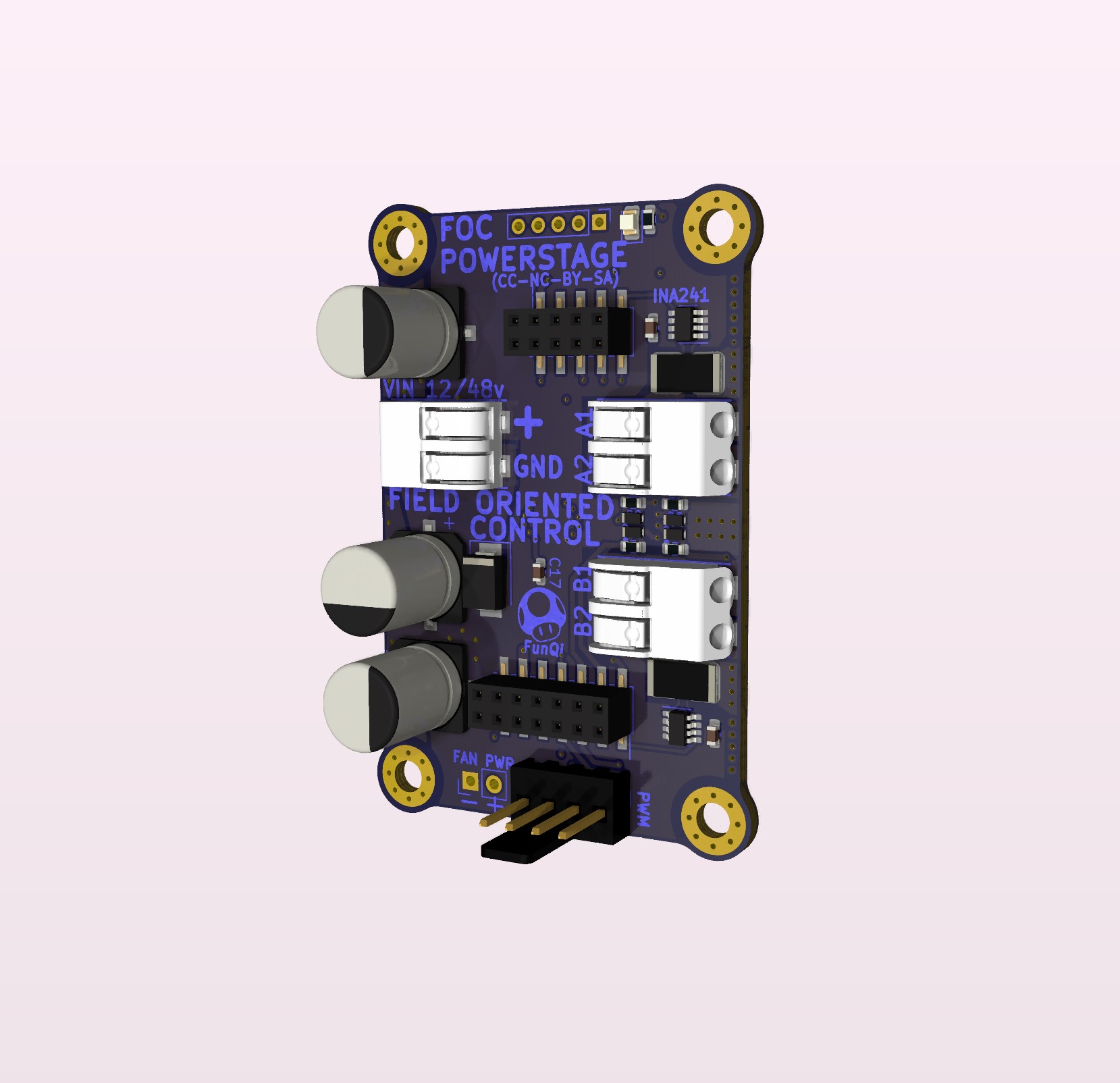
Now that the driver has been integrated into the “MCU-Stack”, the NEMA23 POWERSTAGE is much cleaner. The high side power trace for the FETs is now a almost uninterrupted plane. Furthermore, since there is no need for 12v wires for switching, because of the onboard buck converter, there is suddenly room for a extra electrolytic-capacitor, possibly two (one large per “phase” and a smaller one just because). Getting close…
Also, now that the external FET drivers are out off the way, there is better room for low side current limiting resistor and diode in front of the FETs.
Because there are various power voltages for cooling fans 5v / 12v / 24v I have decided to break out the fan power. The fan header/connector is still relevant because of the PWM speed control, which will adjust the cooling compared to measured heat/temperature development. If using a 5v cooling fan, it could be powered by the 5v USB power. It would then need jumpers from the USB headers to the fan PWR. I will try to break out the regulated 12v for testing on the fan while switching. A Noctua 60mm fan only uses like 0.1amp so in theory it will not drain the power too much. One concern, doing this, is if the 12v fans can handle the 15v the STSpin32G4 buck can output. Raising the switching voltage to 15v could lower the Rds(on) and thereby run the FETs cooler (if the gate can handle 15v).
I am tempted to run the 5V to the cooling fan and make it a closed solder bridge, in order for it to be possible to use 12v, but the 5v would be standard. @runger Du you think it will work, if the CAL_EN pin for the MT6835 was tied to a switch/button ? Hopefully the calibration is a onetime thing and the motor does not need to be mounted to perform it. Its actually a bit difficult to discern, by reading the datasheet, if the CAL_EN shall be toggled or held down?
Just realized that Noctua cooling fans can be controlled by 3.3v.
Edit: Although they probably can work with a 3.3v signal, somewhere I found a dude saying the PWM line is pulled up to 5V inside the FAN. So I am opting for a Schmitt-Trigger (level-shifter).
Note: Since running a stepper using FOC should keep everything cooler then normal (Not FOC), I still think it is a cool feature to have it available if pushing the motors for extended times.
Changelog:
Since this powerstage just as well can drive a 3phase BLDC (Push wire terminals are rated for 9amp), and now there is room for the 3th electrolytic (composite) capacitor, I will go ahead and place it. Keep in mind that they are not that large. They might seem large in this image, but in fact they are quite small (8mm diameter). The lifetime expectancy of capacitors is heavily reliant on how hard they are driven, so adding a 3th large cap will increase the overall lifetime of the other two caps, and will of course increase the overall system performance, especially when driving NEMA34s.
I have made a 2mm pitch header for the CAL_EN pin. This way one can wire the button if needed in some unthinkable scenario where you want to calibrate or re-calibrate the sensor while the motor is mounted on a machine, where it can be hard to access a small button. Naturally the belt or what ever drive train is used has to be taken off, if the motor needs to spin fast and freely during the calibration. One can also wire it to one of the available pins on the MCU stack, if one needs to calibrate often, for some strange reason. Hopefully it is just a onetime event.
Just been looking through this again. Although you a right, the order is different. MISO is channel 1. Was concerned they flipped the order on the two SPI channels, but its ok. Just have to use PD2 for ETR on the Port A SPI interface, since it not present on SCK. Since both SPI1 and SPI3 are present on the Port B interface, it would be nice if we keep that port SPI3 in the pin definitions. Otherwise it might crash with the SPI1 on Port A.
I have tried to mess around with the SlimStack. It is actually possible to have a SPI interface if the MT6835 is turned in one direction and ABZ if the sensor is turned the other direction, this without possibility for short-circuit. See below.
Edit: just checked the datasheet and there is a 250k pull-down on the CAL pin (internally). Further pull-down could be placed on the sensor breakout, so it does not interfere with the SPI lines if turned 180 degrees.
Ok, this is quite cool, but this is pretty confusing for the user, I think…
I think you have to be clear on the goals and make clear specifications, and then decide where to solve what.
The shared SPI/Encoder interface is something specific to the STSPIN32 module you’ve made. It could be a design feature of other STM32s with similar pinouts, and I think also ESP32… but its unclear whether this could work with an NRF52 or SAMD based board…
So I think this is a local problem to be solved locally on the MCU board, not by rotating the sensor.
In my mind the sensor should always connect in the same way, and since its easy to get these board to board connectors with many pins, why not use one with 10 or even more pins, and have standard pins for ABZ, SPI, UVW, error, calibrate, PWM, Analog, etc… You could even add a pin called “ID” - which attaches to a small ROM on the sensor. Then the MCU board can read the ROM data via the ID pin, find out which sensor is attached with which protocol(s), and initialise itself accordingly.
But even without the nifty auto-detect, having a standard pinout with all the signals means the MCU can select the ones it needs, and for example on your STSPIN board you could either connect both SPI and ABZ to the two ports, or make one of the ports selectable between the two using a multiplexer or buffers with OE function.
Nonetheless, the reversible sensor is pretty cool ![]()
Yes, well, I see your point regarding it being confusing for some, it will of course need a detailed explanation and clear and visible indications on the sensor and board. I have faith in the user ![]()
The thing is. One of the ports/sides will be routed to headers on the Powerstage. I need to limit the pin_count on those dual_row headers. So the SPI interface will be standard. If the user wants SPI and ABZ interface, that’s possible using jumber_wires from the Powerstage (ABZ output header) to the MCU stack. Pure ABZ is also possible if the user need the other SPI port for something else.
So if for example the ABZ interface is not on the SPI pins (like the STSpin32G4) if using a MCU stack with a different MCU, then the user has SPI as standard, but also the possibility to interface the ABZ.
I dont remember how it is for the STM32H7…
CHANGELOG
Now the current sense amplifier INA241 from TI is finally available, I have made the jump. This makes the current sense part so much cleaner. Since it can survive 120v I will not place TVS diodes like with the MAX46056. I will still place a large (main) TVS close to the bulk capacitor. This sensor is a real upgrade compared to the MAX40056, although because it is so fast 1100 kHz, not all MCUs are able to read it. The ADC of the STSpin32G4 is fast, so there should be no problem with this combo.
Changed shunt resistors to larger 2010 package 4W rated. The INA241 I could get my hands on are the 10V/V (Gain) one. This means relatively high heat dissipation, but up to 5 amp should be OK, more then most NEMA23 can handle.
Edit: It is always tricky to set the shunt current range, because we want highest possible precision within the application specific parameters. That said, we can still have useful reading in the lower 50% if the result is in 14 or even better 16bit. This entails oversampling in the case of STspin32G4 since it “only” has 12bit native ADC resolution (ADC 4MSPS). Naturally we would like to get close to the wire terminal ratings (9amp), but that is far beyond the range of any NEMA23 even NEMA34 does not usually go that high. We also want some headroom for 3phase BLDC use, so 8 amp sense range is IMO a good tradeoff (8amp @48V = 384w). With that kind of power we can actually drive a small eBike (250w nominal in the EU).
For the uninformed: 12bit is 4096 resolution, 14bit is 16384, 16bit is 65.536, so even in the lower 50% range of 14bit we have a resolution of 4096 in both directions (current flow).
That leaves us with a 18mOhm shunt_resister (with additional margin to spare). Although maxing out the current on that resistor will dissipate 1.2W, which means it will start to get luke_warm.
Maybe 22mOhm is more appropriate for this kind of application ? @Valentine
Edit: Changed to 2512 shunts 7W rated.
I’d go for hall-based current sensors, cold 0R single chip, avoid all that mess with opamps, shunts, and overheating. Each shunt has more resistance that the mosfets they are measuring themselves. What’s the point of spending so much time picking a nice low R mosfet then throwing up all over with a shunt.
Cheers,
Valentine
Its not comparable, since the MOSFETS RDs(ON) is turn_on resistance not resistance in the shunt_sense. In a sense you can say, that the shunt will not dissipate the energie calculated by Ohm, since we PWM the current, like the gate resistor does not overheat.
I would like to do the same board with a Hall-based sensor one day. That would make a interesting real_world comparison.