Schematics can be found here;
Regarding the Clock source; there is a internal 32 KHz and 16/48 MHz clock. The internal 32 KHz clock “only” has 5% precision, so placing a external 32.768 KHz clock is a option. The internal 16 MHz clock has a precision of 1%. I’m guessing STM is using the external 24MHz clock for PWM generation / tick counting ? Setting up the Advanced Timers TIM1 and TIM8 would then require an appropriate divider etc. Maybe the internal 48MHz clock is used.
Usually the 32.768 KHz clock is used for real-time purposes, eg. in a watch. Do you see any need for that in our use case?
TBH I think you’re fine putting nothing at all.
The low speed oscillator is needed in the low power mode, and 5% isn’t very good so devices that need to follow time and wake up after a reliable delay would include an external low speed clock. I see no need for it on a motor controller.
The high speed oscillator is needed when the chip is not in sleep mode, and is used to feed all the other clocks (of which there are many) in very complicated configurable ways. You can use any value you want within a certain range, as the actual (generally higher) MCU master clock frequency is generated via a PLL circuit in the chip.
If this clock is imprecise there can be problems with fast protocols like USB. But I would assume that 1% is sufficient and USB will work with just the internal oscillator.
One of the big advantages of using the same clock configuration as (for example) the Nucleo board for the same chip (in this case the G431 core it uses) is that you can use the board description files for that board. If you change the clocks you have to define your own configuration.
Ok well then 24MHz it is ![]()
Regarding SCREF: They set this to a fixed 1V level in their application example. I thought this was for over-current protection, but it’s not, it checks against shorting to ground. So maybe leaving it as they suggest is fine, or maybe it can be made settable… I’m considering doing this:
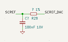
if I find I have a spare DAC pin left after the other stuff. Then I can set it from the MCU using its DAC feature, or just set it to output HIGH to disable the protection. Same component count as the resistor divider…
Yeb, it apparently has several sensitivity settings in its register. At first I thought it was the activation (voltage limit) that would trigger this safety feature, like if the 3.3v went below 2.8v or whatever caused by a short, but it is something more sophisticated. It might actually save a otherwise burned MOSFET…
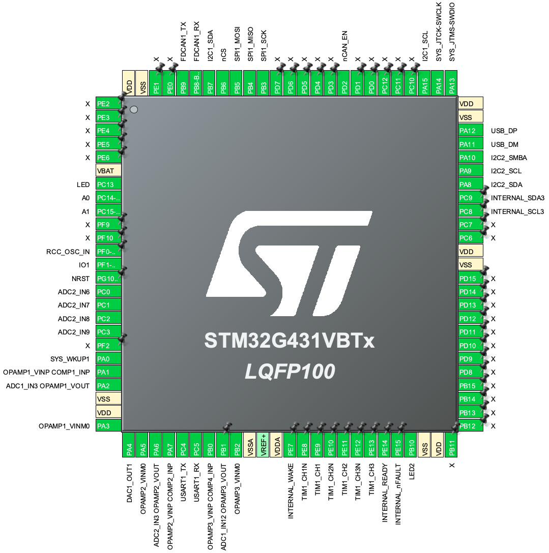
Ok, this is the pinout I have settled on, I hope there are no errors.
I used the G431VBT as basis, and locked all the unconnected pins as outputs (marked X).
I used all the pins on the STSPIN32G4 and have the following:
- SPI bus for sensor, alternatively same pins support an hardware encoder or hall sensors on TIM3
- internal SMBA bus
- external I2C bus + interrupt/wake
- CAN RX,TX and enable
- USB
- UART Serial (will route this to the SWD header for connection to PC via ST-Link)
- SWD
- SCREF DAC output
- current sensing
- voltage sensing for phases and Vbus
- 2 LEDs
- 2 I2C address selection pins (or general inputs)
- 1 IO, general purpose
- NRST, BOOT0 (with CAN_RX)
For BOOT0 my strategy is to keep the CAN chip disabled via pull-up during power-up, and only enable it by the MCU after boot. In shutdown mode the chip keeps its RX and TX lines in high impedance. I have made the pull-down resistor on BOOT0 very high-valued, and omitted putting a filtering capacitor on it so as not to stress out the CAN_RX.
Sweet, I will try to play around with the STM32CUBE_MX, first time creating such a project.
Since I do not intent on using the COMP etc. for current sensing, but rather rely on external inline bi-directional PWM immune sensors, the setup will look a bit different. This choice mainly comes down to minimizing pin-count on the bottom dual-row headers. As I understand it CUBE_MX generates some basic init file(s) ?
In ADC1 there appears to be a internal temperature sensor (thermistor). Did you activate that ?
It generates a bunch of code, but all based on STM32s HAL. Not so much use for Arduino framework. But you can use their clock setup function if you correctly configure all the clocks…
But it’s invaluable to do and check the pin assignments. Otherwise, with so many pins it’s very hard not to make mistakes.
If you want to use similar pins to mine then it will be easy to share code later, but its not a big deal if the pins are different either.
Sure is, just realized that the FAN PWM pin should be on a separate timer, in order to generate the frequency / waveform needed to control the fan, so will change that from PC3 which only has TIM1, to eg. TIM4 on another pin.
Regarding the HARDWARE SPI NSS (Slave Select) Pin; somewhere it is written that it can have a weird behavior and that it should be set up as a GPIO for proper compatibility?
Really? Well my pinout doesn’t use the HW CSS pin I don’t think. But even if it does, you don’t have to configure it as such, you can just use it as a GPIO.
you don’t have to configure it as such
Yeah, no worries.
I see you enable the SYS_WKUP1? I suppose it wakes up the system, but how do you intent on using it ?
That’s a good question:
One use is from I2C: one control concept (which is quite simple to use) is to control the driver via I2C, for example via our I2CCommander classes. I put a Stemma/QT compatible JST SH port on the board for this. I add a 5th line for WAKE/INTERRUPT functionality:
- when the driver is asleep I use it as the WAKE input
- when the driver is running it is the INTERRUPT output - for example to signal things like movement completed
At the moment I’m using a CAN transceiver that supports only shutdown, but there exist ones that support wake-up functionality. With such a transceiver the WAKE input could also be driven from CAN.
I’ll also make a solder pad for it, so people can attach a button or other external source of wake-up.
OK, I see… PA0 is a fast ADC channel I’m sure you know. If broken out like that, it could also function as a ADC input, unless you pull it up/down. PC5 and PC13 also has WKUP functionality.
Edit: Good point regarding the TIM3 and the possibility for Hardware Encoder interface if not using the SPI1 interface. This does require not to use the Hardware SS ( Slave Select) pin since only TIM3 channel 1 and 2 are present on the Hardware SPI pins. Will TIM3 channel 1, 2, and 4 work in combination as a Encoder Interface? Perhaps Channel 4 as Z (PB1). I see it is the same for SPI3.
The encoder interface uses channels 1 & 2 for A and B and the timer external trigger (ETR) signal for the index. I believe those are the pins I have for MOSI, MISO and SCLK…
Oh, Ok. I believe you, but I’ll most likely double check that.
Edit: You are absolutely right
The third encoder output which
indicate the mechanical zero position, may be connected to the external trigger input and
trigger a counter reset

Hmm… this means Ill have to use PD2 as SS (Slave Select) for SPI1, If I want to enable that feature on the dual-row header plus the SPI3 which is broken out on the side-header, essentially making it possible to have a SPI rotary sensor connected on SPI1 and a Quadrature Encoder sensor w. Index pin connected on SPI3 (or the other way around).
Or just leave it, since its already on the SPI3 (side-header/solder header)
PC13 can only source 3mA. Så driving a LED on that pin is not recommended.
Driving a RGB led w. seperate power is another story. Just be mindful of this.

Regarding the JTAG SWCLK (TIM8_CH2 (PA14)) pin as GPIO. This pin is pulled low on/after reset. So using that pin for FET driver HI/LI should work, I think. When releasing the pin after reset it should be pulled-down immediately or rather stay pulled down.
![]()
Hey, thanks for pointing that out! While I run my LEDs dim it’s obviously best to follow the datasheet here so I’ll drop the second LED and make do with one… I’ll make it another address selection pin instead.
Regarding the SWCLK pull-down, it is probably wise to put 100K resister on it just in case it floats at some point between reset and pin setup. The same for the other control line on the 4th bridge. All the control lines related to driver control inside the STSPIN234G are pulled low.
A 100K resister should not disturb the SWCLK functionality, since 10K to 100K is normally recommended, if the lines are not pulled-low internally.
