High Voltage and Battery Safety
Suggestion:
Be aware, that this high DC voltage can be a challenge. If a fault causes a short circuit, the battery may be able to support very high currents, which could lead to arcing and fire risks. So you need good sand fuses in series with the battery to prevent some nasty events.
Response:
Thank you for the important reminder. Yes, I’ve placed a fuse in series with the battery wire. During earlier testing, I was using the same setup. Still, I appreciate the suggestion — safety is crucial in high-voltage systems, and it’s good to be reminded of the risks involved.
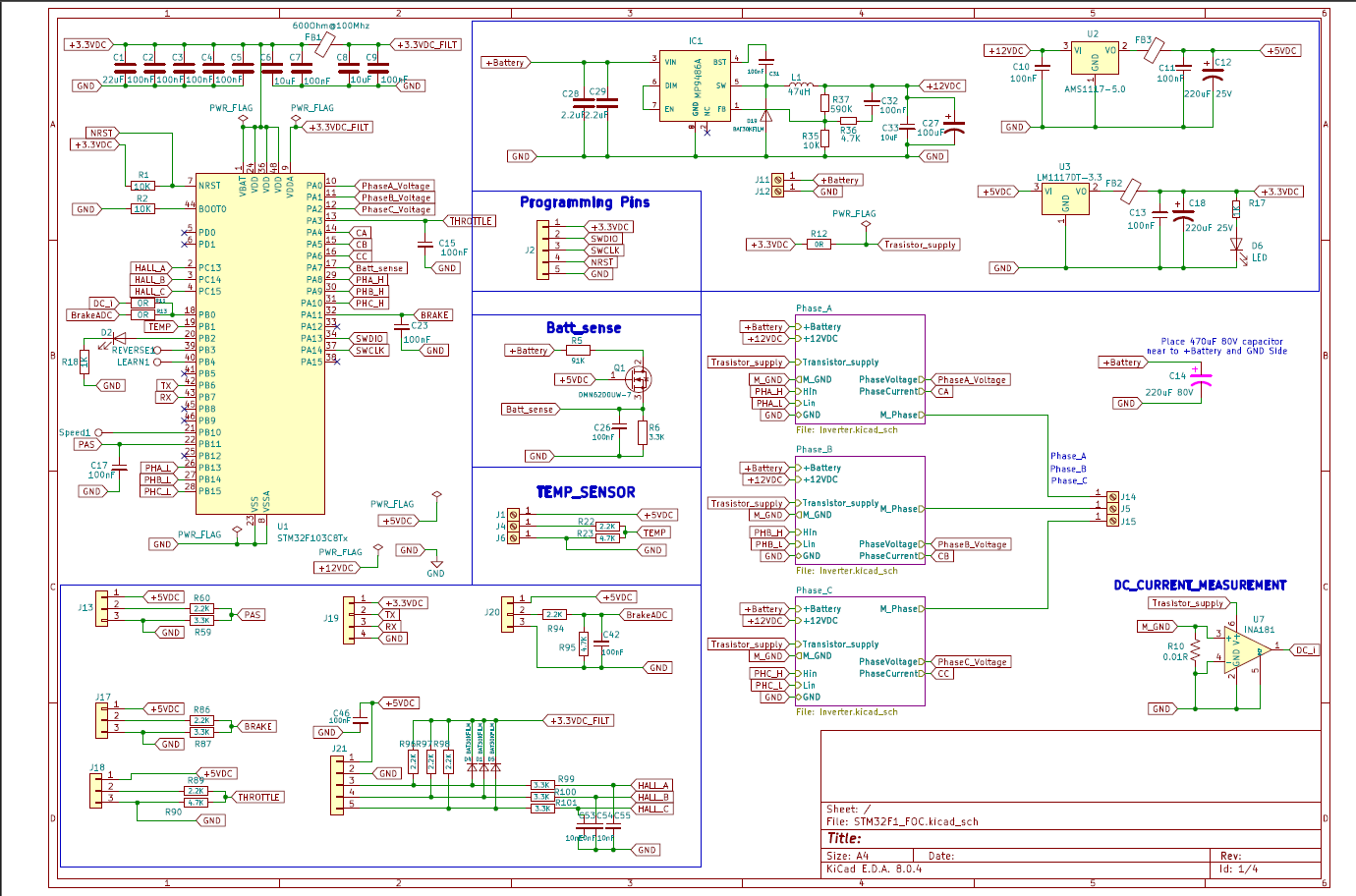
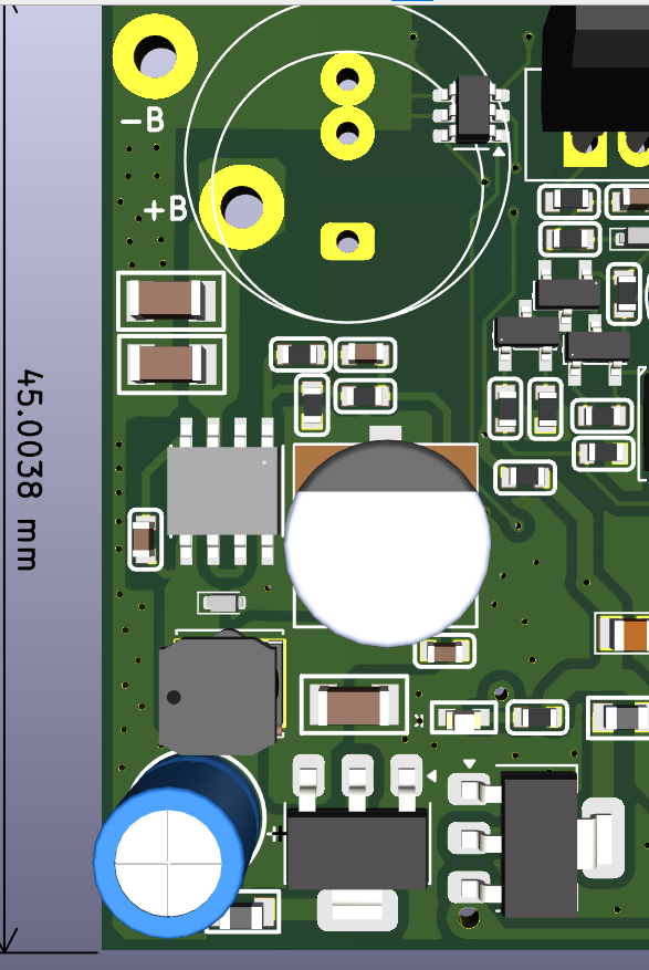
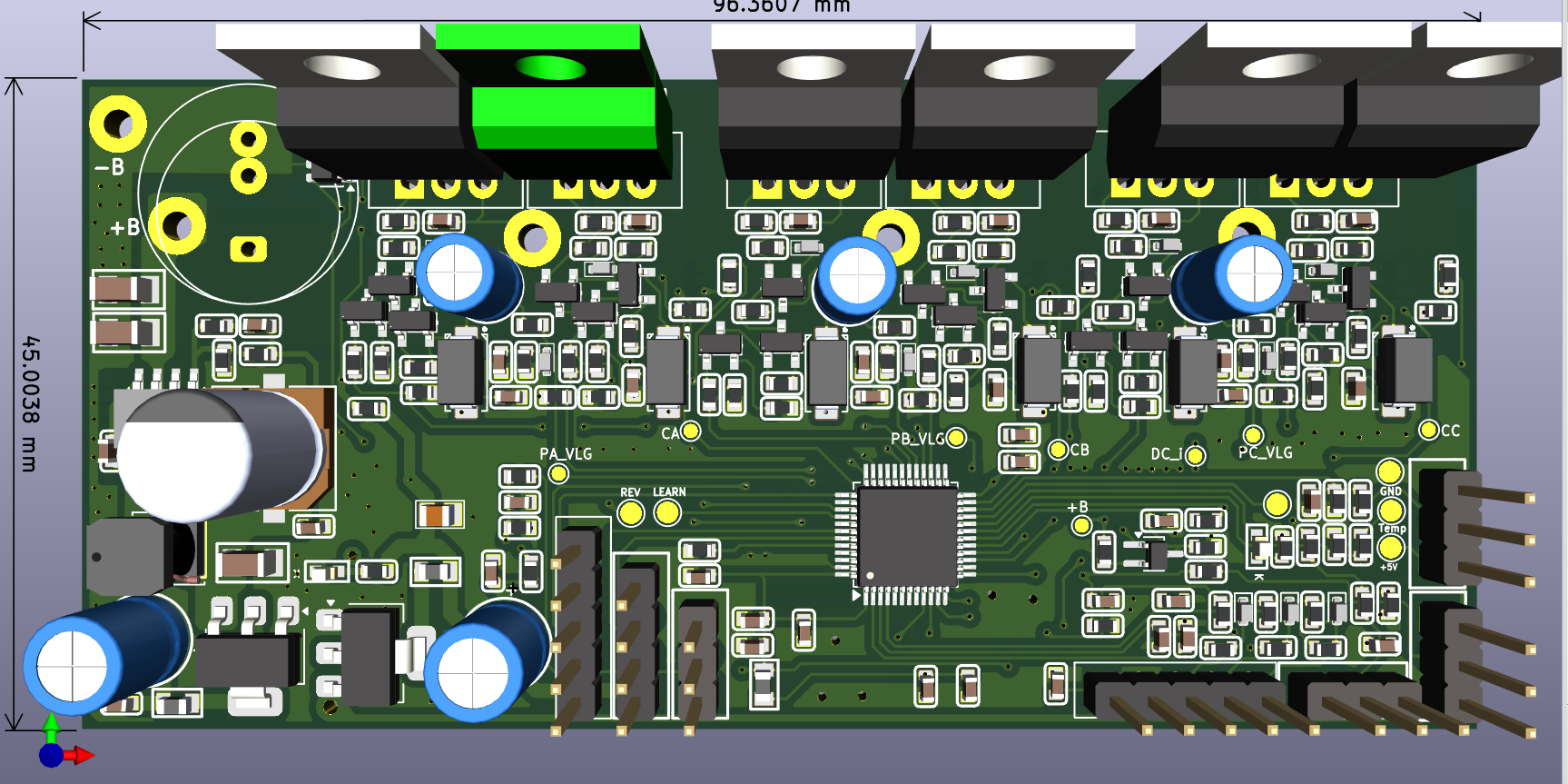
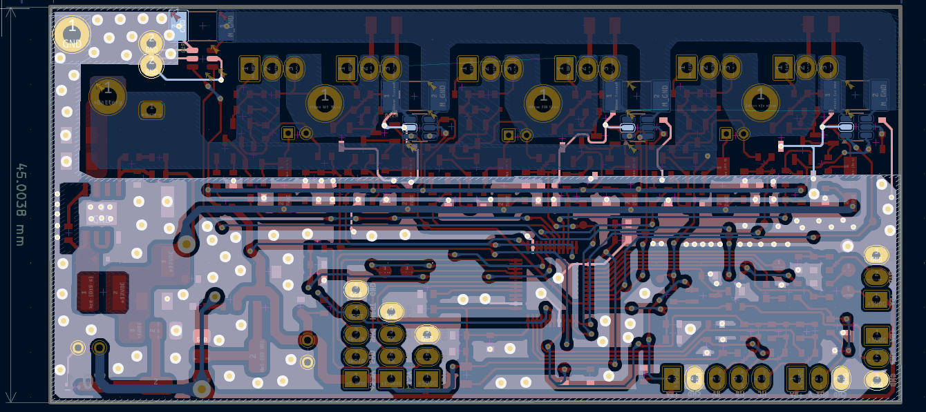
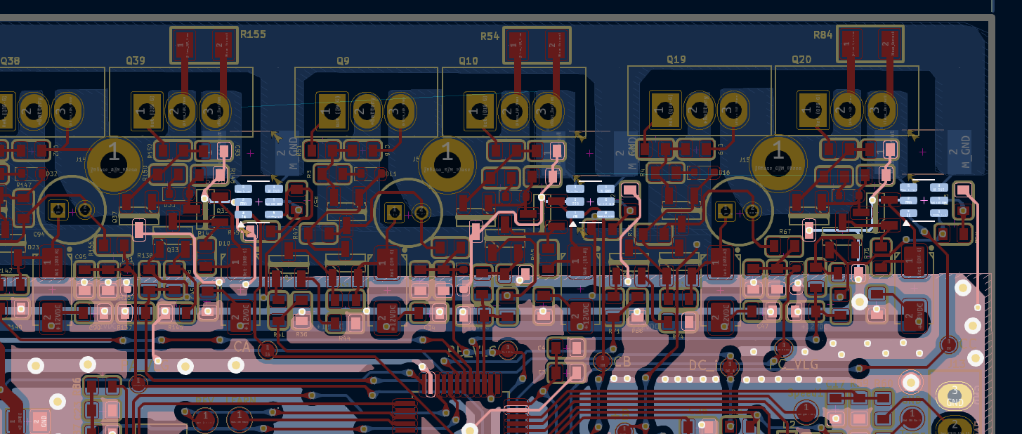
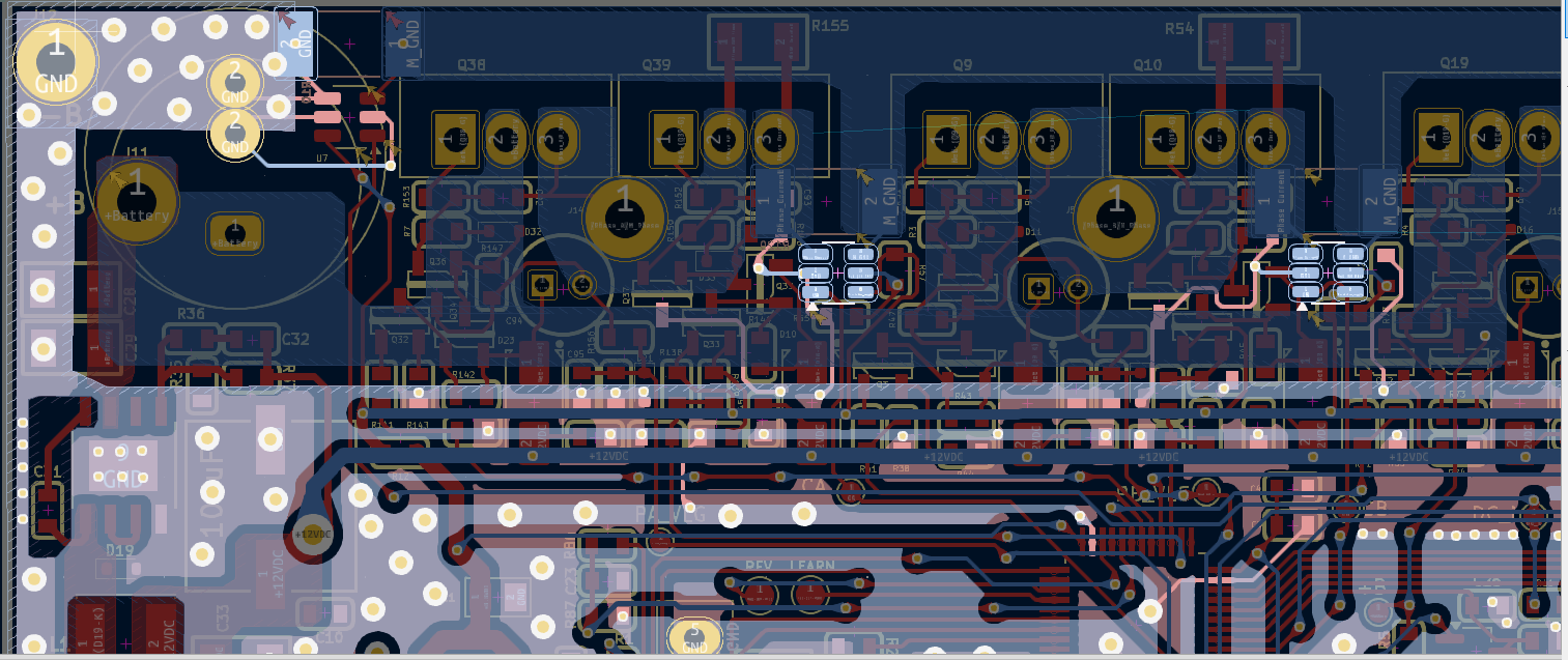
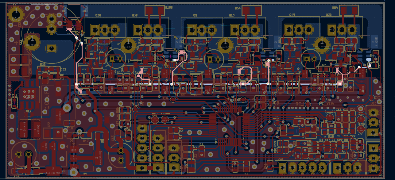
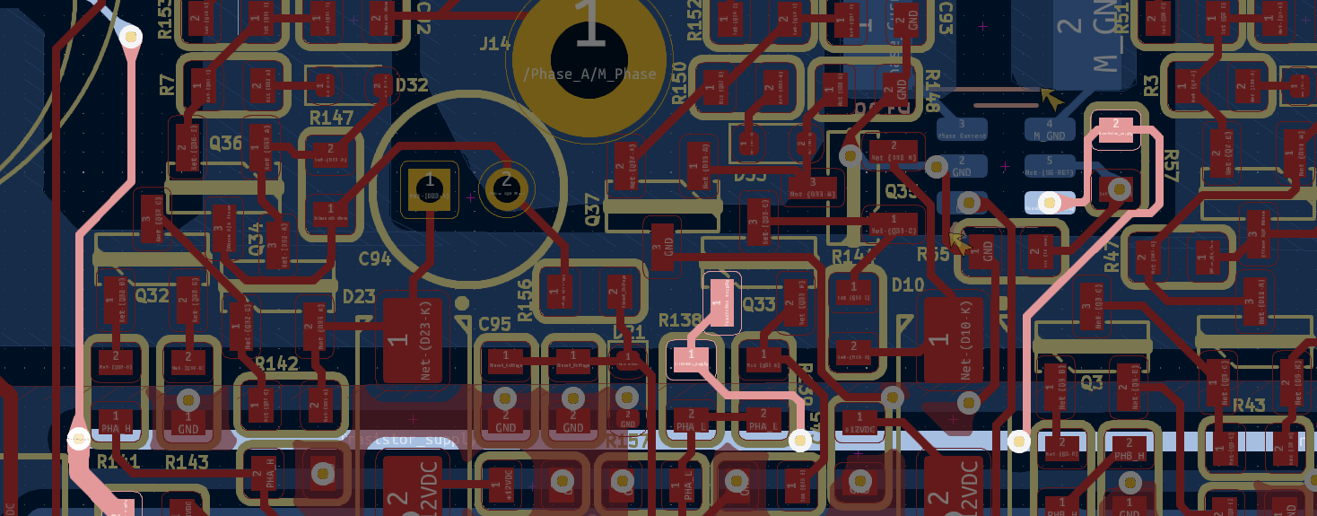
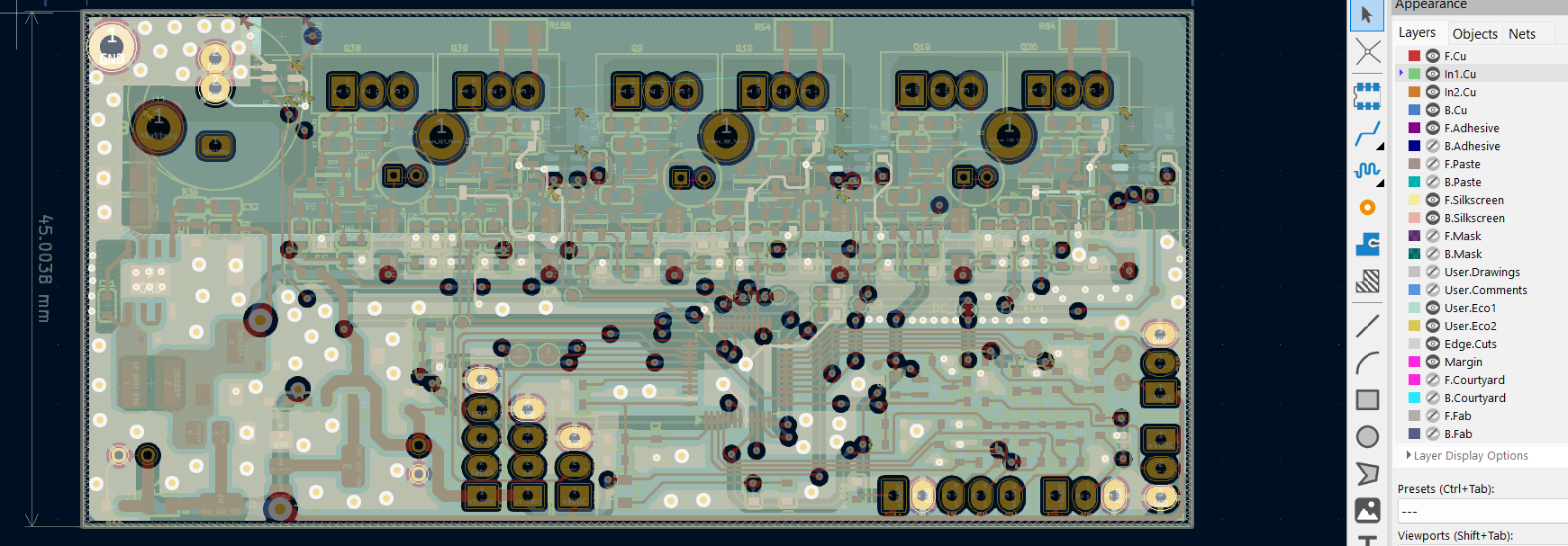
Common Shunt and Self-Inductance
Suggestion:
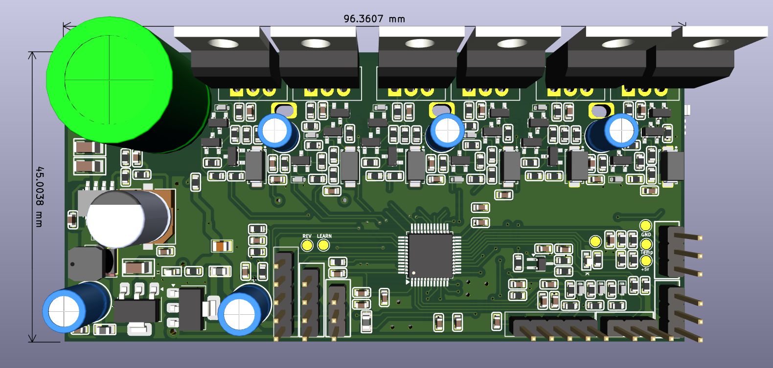
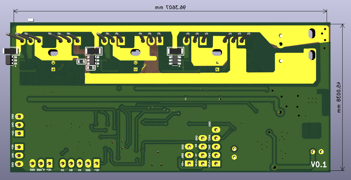
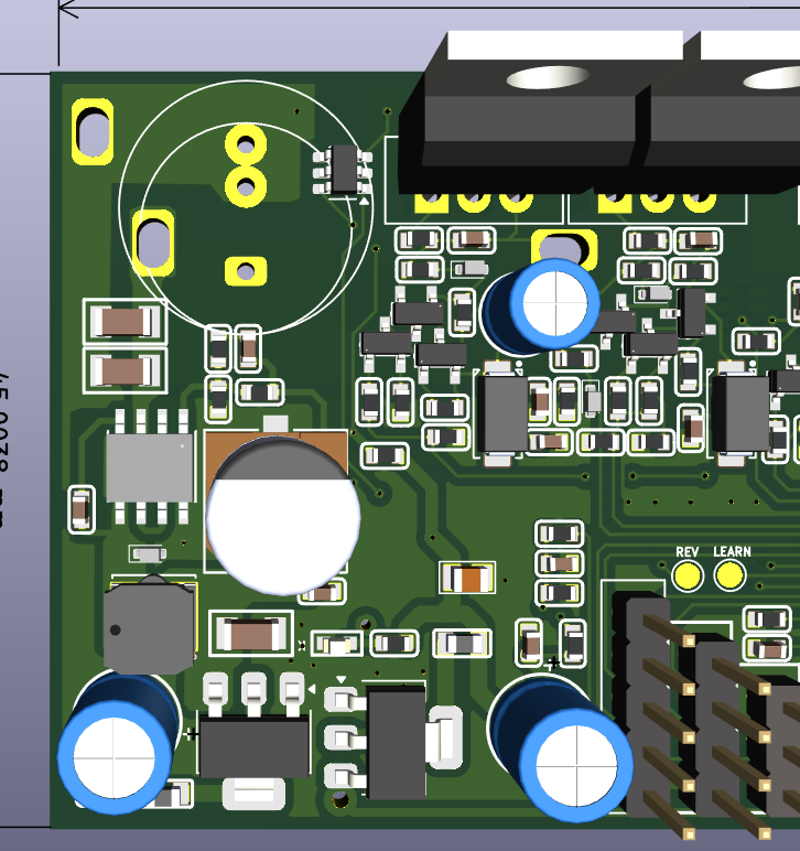
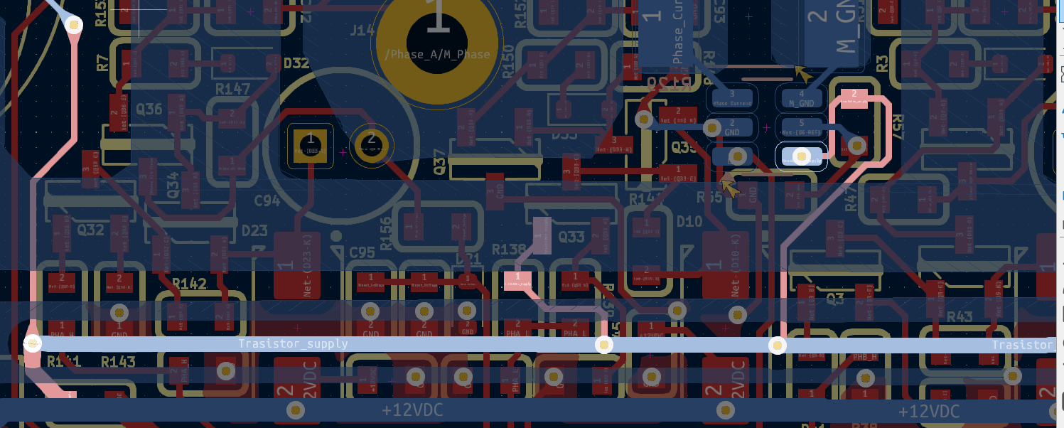
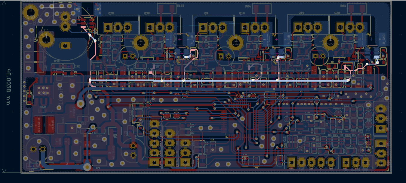
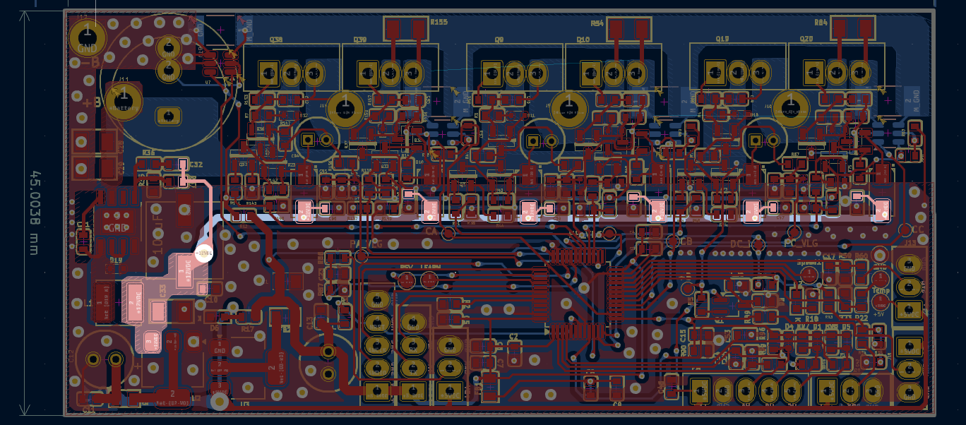
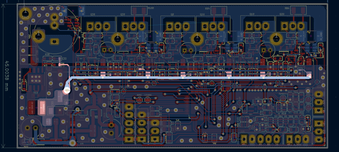
I would avoid the extra common shunt resistor, because it introduces increased self-inductance of the ground current path. You can measure the current in the three phase shunts and sum them instead. I also dislike the self-inductance from the large electrolytic capacitor to the distant half-bridge. In the previous design, a ground path on the other side of the PCB helped. It would be better to have two electrolytic capacitors, one at each end of the PCB, to reduce this inductance. While it might make the board longer, the overall height could be reduced.
Response:
Thank you for the detailed feedback. I am planning to implement both sine commutation and FOC.
-
For sine commutation, I intend to remove the three phase shunts and use a single DC shunt.
-
For FOC, I will revert to three phase shunts and remove the DC shunt.
I also agree with your observation on self-inductance and layout concerns. Based on your suggestions and input from Dekutree, I’ve decided to go with a 4-layer PCB, which should help significantly with signal integrity and grounding. In some parts of the layout, I was indeed struggling to provide proper ground paths, so the extra layers should help resolve that.
Shunt Resistor Value and INA181 Output Swing
Suggestion:
I think you will want to measure ±15 A with the shunts. This is 0.15 V across a 10 mΩ shunt. The INA181 has a minimum gain of 20, so this causes ±3 V output. But the INA181’s output range with a 3.3 V supply is only ±1.65 V, so I suggest 5 mΩ shunts instead.
Response:
Here are the output swing calculations for different shunt values:
 Case 1: 5 mΩ Shunt
-
Vshunt = ±15 A × 5 mΩ = ±0.075 V
-
Output = 1.65 V ± (0.075 V × 20) = 1.65 V ± 1.5 V
-
➜ Output range = 0.15 V to 3.15 V 
Perfect fit — fully utilizes the INA181’s swing range without clipping.
Yes, you are absolutely right. This is the ideal choice.
Case 2: 3 mΩ Shunt
-
Vshunt = ±15 A × 3 mΩ = ±0.045 V
-
Output = 1.65 V ± (0.045 V × 20) = 1.65 V ± 0.9 V
-
➜ Output range = 0.75 V to 2.55 V
Still valid, but reduces ADC resolution.
This comparison confirms that 5 mΩ is a well-balanced choice for maximizing resolution without risking output clipping.
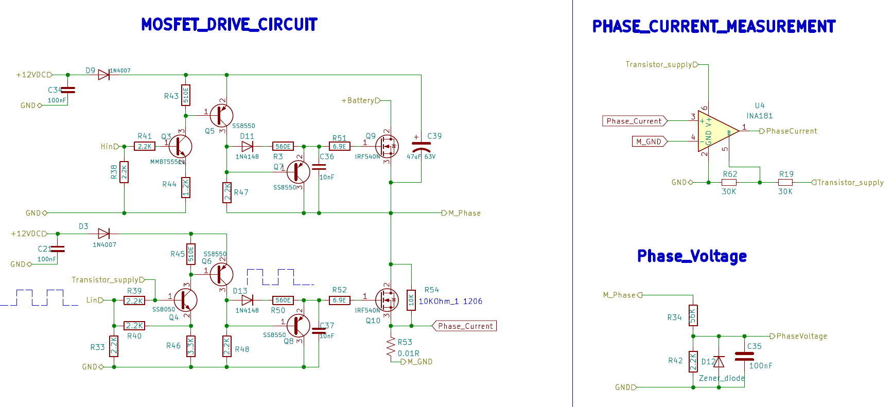
CMRR and Reference Input Impedance
Suggestion:
You want good common-mode rejection (CMRR) with the INA181. It’s rated at ≥84 dB with zero Thevenin impedance on the reference pin. But R19 and R62 form a 15 kΩ resistance, and with the INA181’s internal 500 kΩ resistor, this drops CMRR to ~30 dB. I suggest reducing those resistors to ~1 kΩ or using a low-impedance reference source.
Response:
Thank you for pointing this out — it’s an excellent observation. I’ve replaced R19 and R62 with 2 kΩ resistors, so the total Thevenin resistance is now 1 kΩ, significantly improving CMRR. I had overlooked this detail initially.
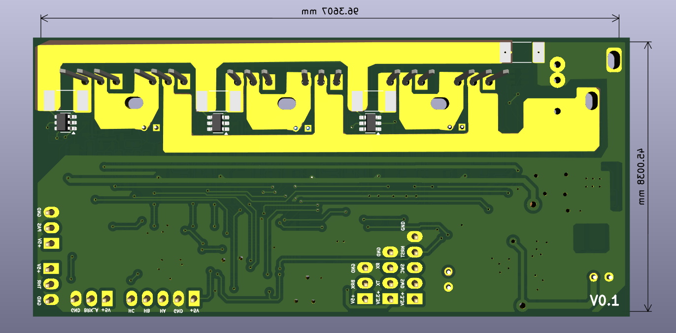
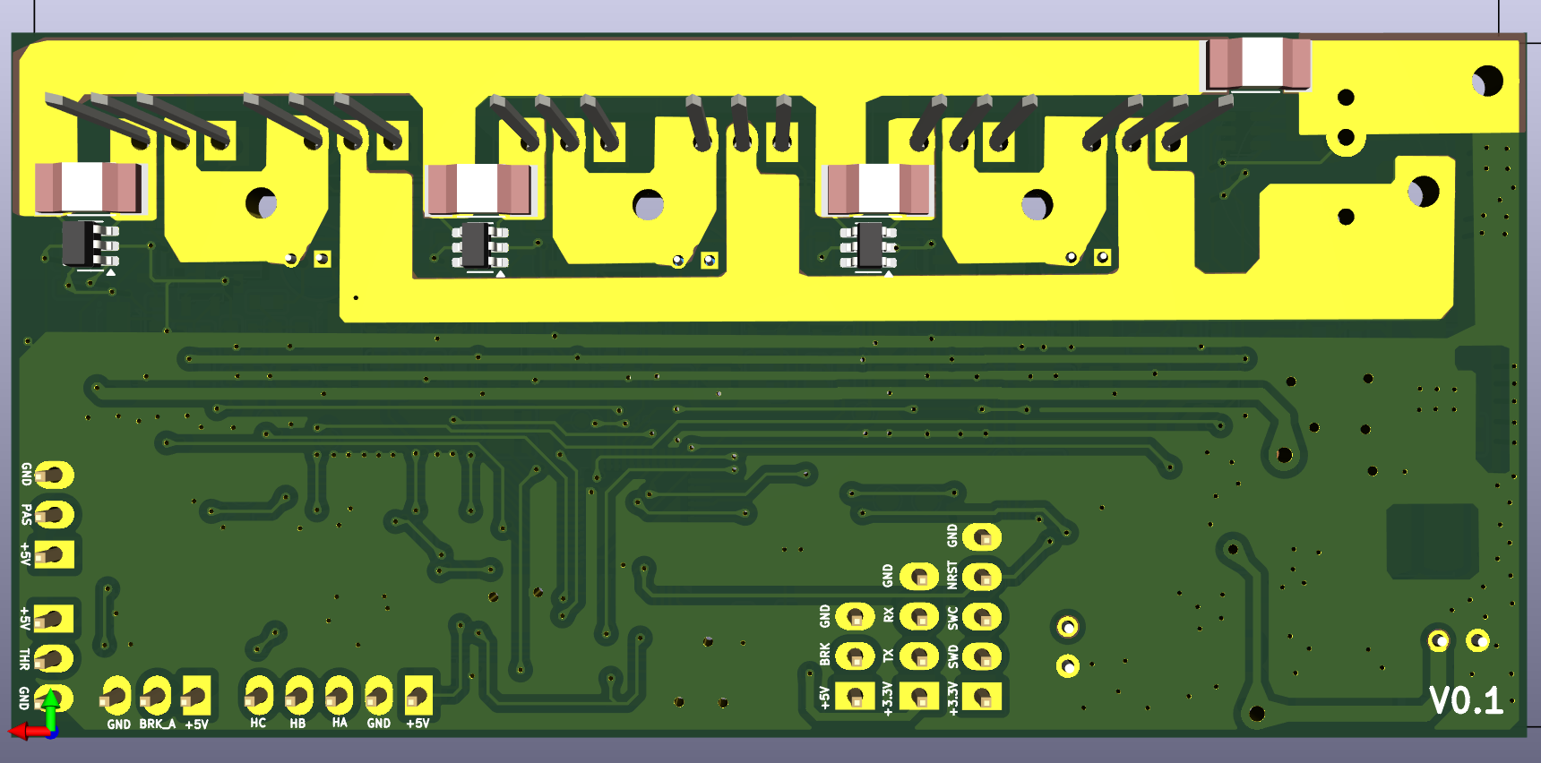
Layer Stackup and Signal Integrity
Suggestion:
I’m not experienced in ESC PCB design, but I know signal integrity improves significantly with a dedicated ground plane. With 4 layers, you can also reduce self-inductance in shunts, which helps minimize high-voltage transients. You may also benefit from RC filtering. If you place GND on layer 2 and power on layer 3, using two electrolytic capacitors becomes easier.
Response:
Yes, I’m moving forward with a 4-layer PCB, thanks to your suggestions and insights from Dekutree. I was facing issues with proper grounding on some components in my 2-layer design. The 4-layer approach will also help minimize parasitic inductance and improve layout flexibility.
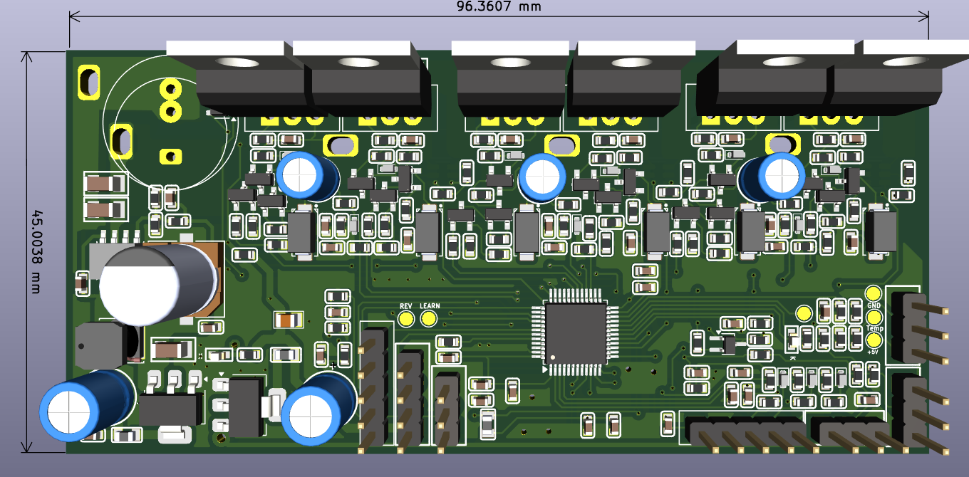
MOSFET Selection
Suggestion:
The IRF540 is widely available but quite old. I prefer something with lower Rds(on) to reduce power loss and possibly avoid a heatsink. Consider alternatives like IPP180N or IRF8010.
Thank you for the MOSFET suggestions. I’ve already shortlisted a few options and will share them shortly for feedback. Reducing conduction losses is a high priority, and I agree — using a more modern, low-Rds(on) device will improve efficiency and thermal performance.