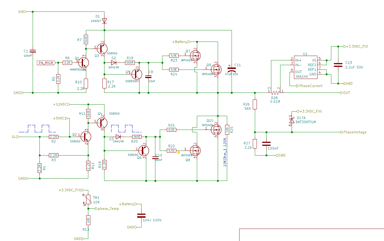
You may want to compare your BAT_SENSE protection with the schematic of the B-G431B-ESC1 (I would send an image, but I am not at my PC right now). It uses two diodes on the MCU pin. The exact type is probably not so important. I think your version is suboptimal.
Thank you both for your questions and answers, it’s very educational to read along ![]()
Hmm, I checked the schematic and it only shows one diode, but it is connected differently. Looks like if the sense pin goes above 3.3v, the diode conducts to the 3.3v power rail. I assume the idea is that all the capacitors connected to that rail would eat the injected power, assuming it’s only a transient event.
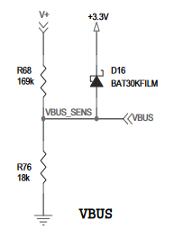
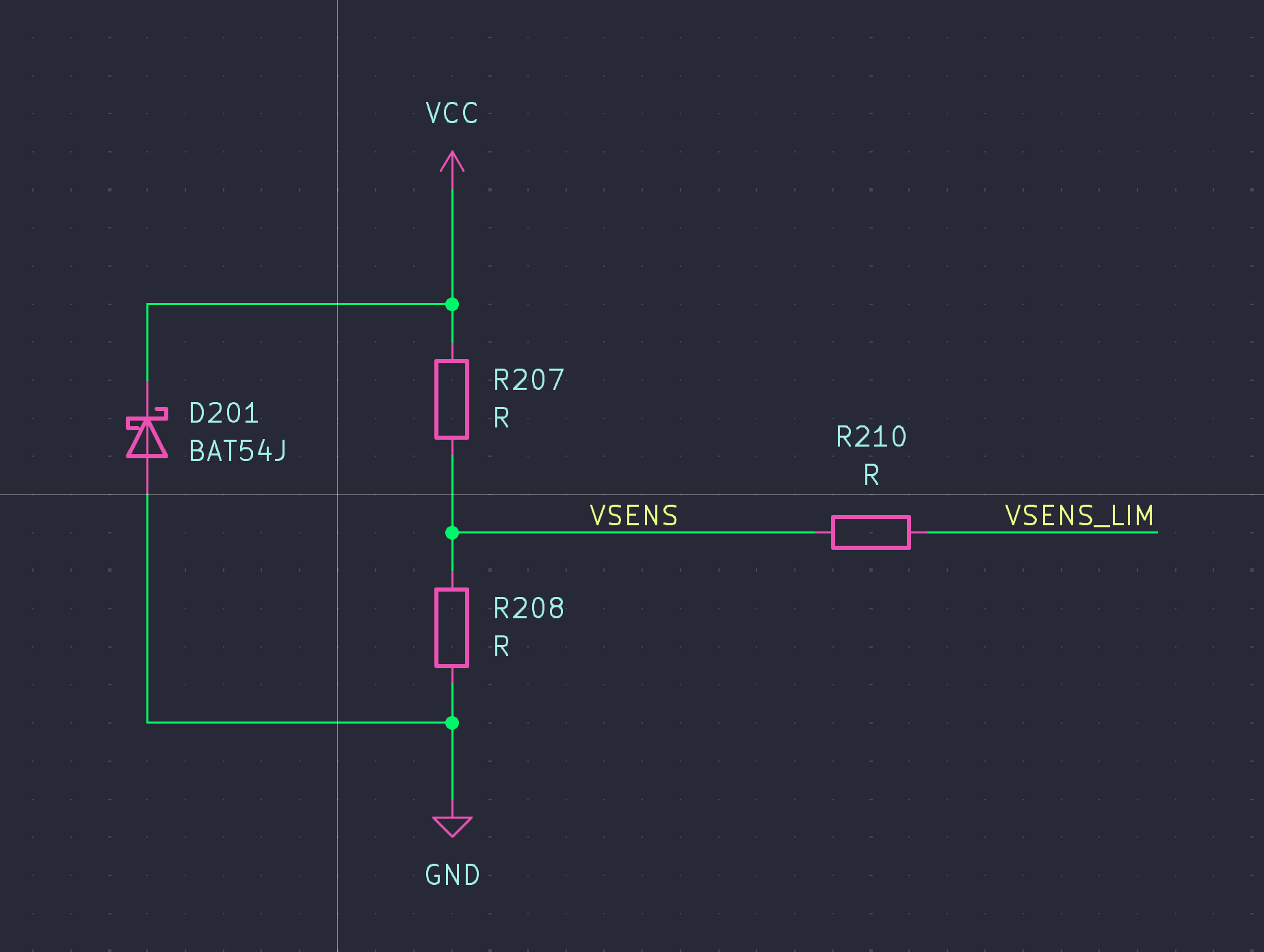
Ups, indeed, you’re right. For Vbus you probably don’t need the second diode between VBus and Gnd, my mistake.
Hi everyone,
@Rikky – Thank you so much! You’ve saved me a lot of time, and I’ve also learned something new from your input. I wasn’t aware of this earlier, and now designing the schematic has become much easier. I’ve made the changes based on your suggestion—really appreciate it!
@Grizzly – You’re absolutely right! I had placed the diode in the wrong direction. I’ve updated it now. Thank you for pointing that out!
@dekutree64
As for the part about the BAT_SENSE protection:
“I checked the schematic and it only shows one diode, but it is connected differently. Looks like if the sense pin goes above 3.3V, the diode conducts to the 3.3V power rail. I assume the idea is that all the capacitors connected to that rail would absorb the injected power, assuming it’s only a transient event.”
I’m still a bit unclear on exactly how that works. Could you please explain a bit more?
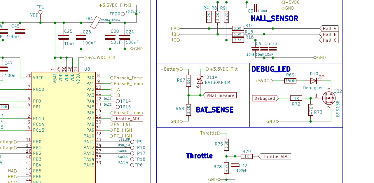
For communication, I’ve currently placed a test point to help reduce the PCB size.
As of now, I plan to use only UART.
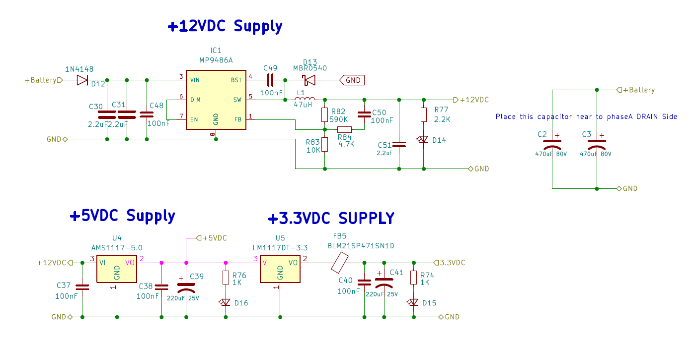
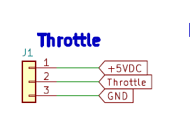
I had made a mistake earlier with the throttle supply, it was set to +3.3V DC
I’ve now corrected it and set it to +5V DC and at throttle output using voltage divider I making it +3.3VDC for MCU compatible.
The diode prevents current flowing from the 3.3V supply to the sense pin (otherwise it would be pulled high and unable to read anything), but if the sense pin goes above 3.3V then current will flow into the 3.3V rail and cause its voltage to rise. That would be bad if it goes on long enough that the capacitors can’t absorb all the energy, but could conceivably protect the MCU pin from overvoltage if it’s only a brief spike.
But running the numbers, that voltage divider with 56k and 18k resistors will only go above 3.3V if the bus voltage is >34.3V, and the MCU pin would only be damaged above 37.4V. And according to Grizzly’s past experience, ESC1 will die even if the bus voltage goes above 24V, so that diode seems pretty superfluous in this case.
Your voltage divider with 56k and 2.2k needs >87V bus voltage to go above 3.3V, but since you’re reading the divider output with PB12 which is 5V tolerant, you’d need >132V bus voltage before the pin is damaged, and your mosfets would be long since dead by then. So I think the diode is superfluous for you as well, and a liability since it could potentially cause the 3.3V rail to rise above 3.6V and kill the MCU before PB12 would be damaged from reading the unprotected divider output.
I believe the diodes should be this:
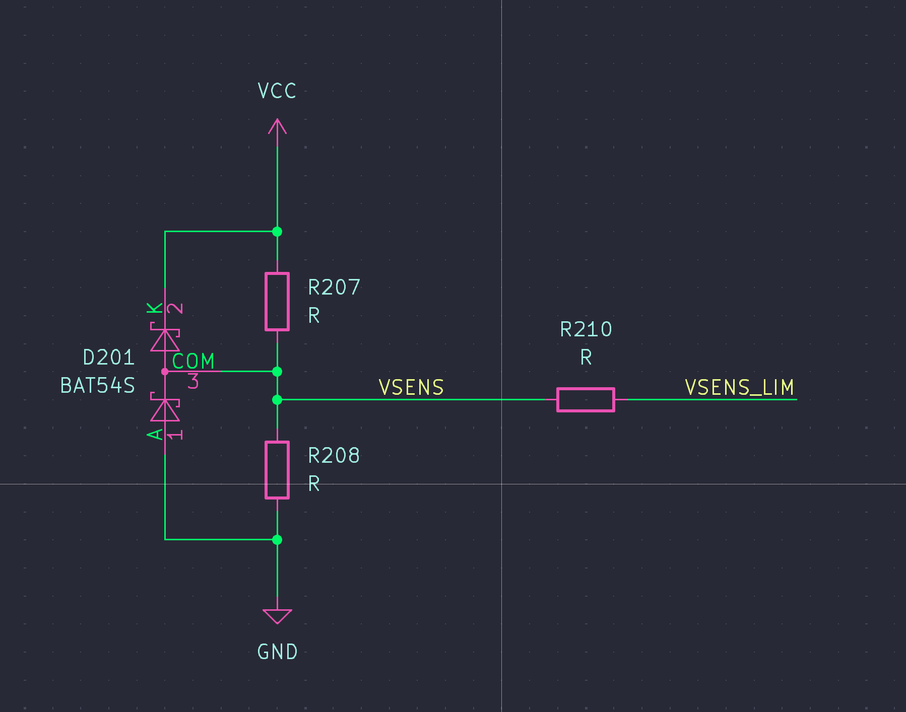
If a spike on VCC occurs and even the divided VSENS is pulled up to high enough to break the barrier, lower side didode will conduct, direct excess current to GND and clamp the VSENS at a safety level.
The higher side diode is used for the same reason, but to prevent spike on GND. When GND level goes bellow a certain threshhold. If we have only one common GND, we can ignore it
I designed this too many time with TVS diode for USB ports, but too dumb to aware that BEMF to power is the same phenomenal.
Hmm, I think I understand the ground diode. So something like this should work for 5V tolerant pins? There’s also this which has 3.32V-3.53V breakdown voltage so should be safe for 3.6V pins, but 3.32V seems quite a small margin from unintentional breakdown.
Would the high diode’s breakdown voltage need to be changed depending on VCC?
I think in most cases, we can use like this:
I am not peaky on choosing the diode at the first board revision though, generally I will do measure the BEMF constant of that specific motor before decide
The correct circuit IMHO is the one with the single diode posted above by @dekutree64.It can be extended by a second diode to Gnd. The latest two schematics miss that we are dealing with two different voltages, Vbus and 3.3V. On the other side, @dekutree is correct in his analysis that with the given resistors, there is a really big margin before th elimits are exceeded (if his math is right which I trust without checking it). At the end, if you need it or not will depend on the resolution and range of the Vbus measurement (defined by the voltage devider) and the expected BEMF.
Hello everyone,
Apologies for the delayed response — I was caught up with some personal matters.
@dekutree64
Thank you so much for the detailed explanation — it really helped clarify things!
You’re absolutely right: the resistor divider already keeps the voltage well within safe limits for the MCU, and using a 5V-tolerant pin like PB12 adds an extra layer of safety. I hadn’t fully considered that the diode could potentially backfeed current into the 3.3V rail — that’s a great insight.
I also appreciate you crunching the numbers and comparing the 56k/18k and 56k/2.2k divider setups. That makes it very clear that the diode isn’t just unnecessary, but might actually complicate things. Simplifying the circuit by removing it seems like the smarter and safer approach.
@Rikky
I’m a bit unclear about how the ground diode works.
When there’s a negative voltage, does it go through the low-side diode? Also, I’m not fully sure how the single diode configuration you mentioned works — could you please elaborate a bit more?
@Grizzly
From what I understand, BEMF increases both with motor speed and when the motor suddenly stops.
Here are the two cases I’m aware of:
- When the motor is spinning at full speed (especially if driven externally), VSENS shows the maximum BEMF.
- When the motor is rotating and is suddenly stopped (again, possibly by an external force), there’s a sharp rise in BEMF.
If there are any other situations where BEMF increases significantly?
I’m still a bit unsure about the best approach — should I include a diode on the high side or low side just to be safe, or is it better to leave it out entirely? Any guidance on this would be really appreciated!
-BldcLover
Hi everyone,
I hope you’re all doing well!
I’m trying to deepen my understanding of low-side current sensing in motor control applications, and I could really use some help clarifying a few points.
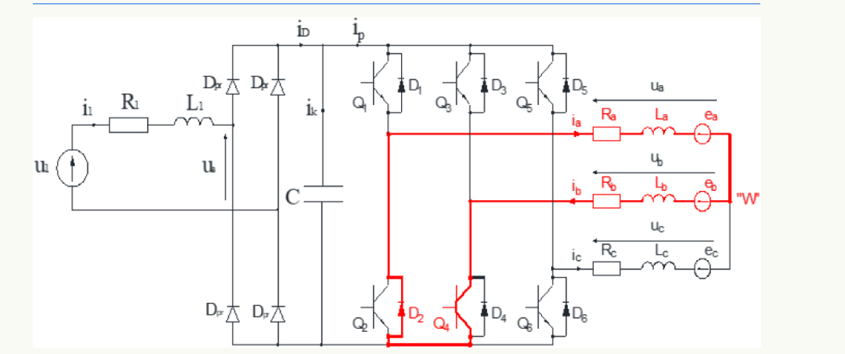
Specifically, I’m a bit confused about how negative current is sensed in a typical three-phase inverter setup.
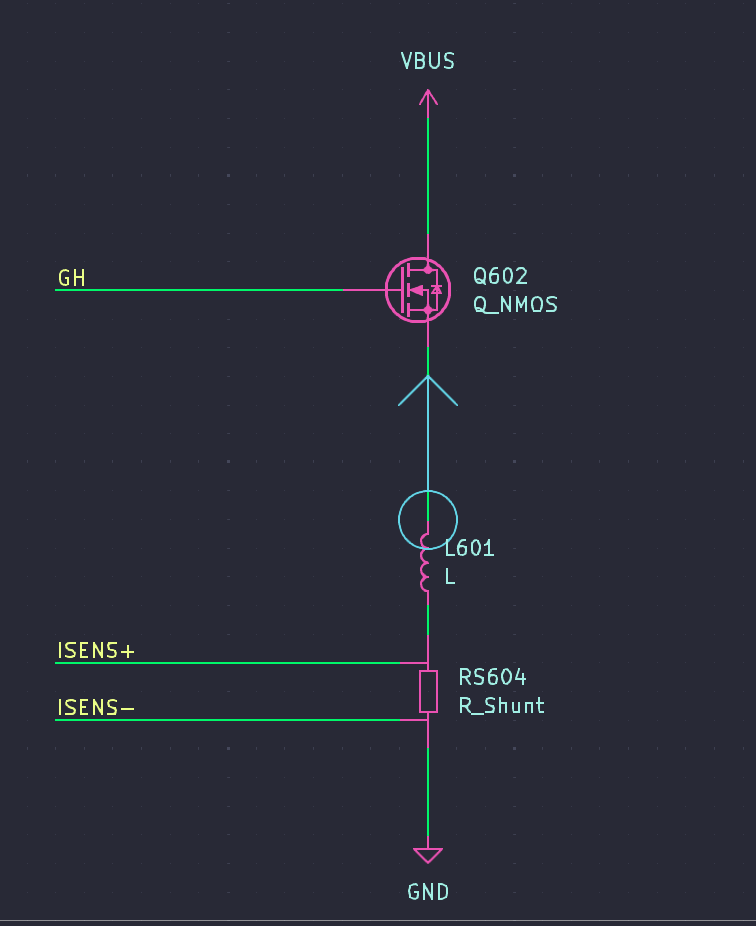
When the motor is connected to the three phases, how exactly does the negative current flow, especially when it involves the MOSFET body diodes? My fundamentals are a bit fuzzy here.
I’d really appreciate if someone could walk me through the current path during negative current flow.
Also, how does the op-amp or current sense amplifier detect this reverse current? and how does the amplifier handle negative voltage drop across it?
Any insights, diagrams, or explanations would be greatly appreciated!
Best and regards,
BldcLover
Hi there,
Specifically, I’m a bit confused about how negative current is sensed in a typical three-phase inverter setup.
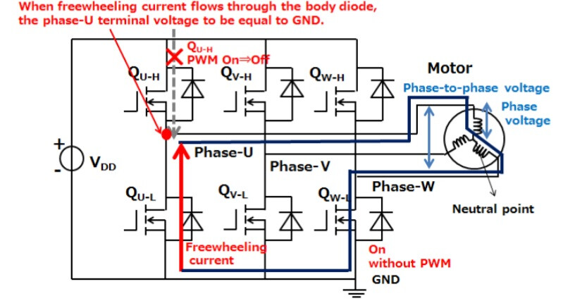
You can simplify it by thinking about driving a simple selenoid load at highside.
The low side should not see any current in this case. Negative current will run from the motor lead to power source through body diode.
Hi Rikky,
I’ve studied this quite a lot, but I’m still having trouble imagining how it works in real time. Could you please confirm if my understanding is correct?
Let’s say Q1 and Q4 are ON, and Q2 is OFF — in that case, will the negative current flow through Q2’s body diode from ground ?
-BldcLover
Ah hah! Now I know why you get confused! I’m not an expert though, so please correct me if I’m wrong.
In your situation, Q1 and Q4 are on, while other are off, basically (I mean just basically, we’ll have an exception) there are no reverse current at all. In this case, the current flow from power source through Q1, to the motor phases, to Q4 and back to ground as normal.
The fun part begin when we suddenly turn off the Q1.
First, the current fed to the motor coil from Q1 source is rapidly decreased. But the coil is, well, the coil. It hates the dI/dt, so it introduces a reverse voltage to resist the decreasing current.
In most case, if dI/dt is high enough, so the reverse voltage will be higher than the power source voltage, thus, there will be a current flow from the motor coil lead, to the Q1 source, through the body diode and back to power source.
Since we will drive the mosfets with PWM, so the on/off scheme will appear frequently, thus we will see the reverse current
Hi Rikky,
Apologies for the delayed response — I’ve been feeling unwell recently, which led to a slight delay in my work.
In the meantime, I’ve been studying more, and based on my understanding, due to MOSFET switching, the motor doesn’t accept an instant change in current. As a result, reverse current may flow from ground to the motor phase — is that correct?
I’ve attached an image to illustrate what I mean; could you please let me know if my understanding is accurate?
I’m particularly confused about how the low-side MOSFET behaves during switching, and how exactly the shunt resistor measures current in this scenario.
Looking forward to your insights. Thank you so much for your time and help!
-BldcLover
Hello everyone,
I currently have a 250W electric cycle motor, and I’ve decided to design a controller in the 350W–500W range, instead of going for a heavier 1kW setup as I initially planned.
My goal is to first understand the fundamentals of Field-Oriented Control (FOC) in both hardware and software with a smaller-scale design. Once I’m more confident, I plan to move on to developing a 1kW or higher power board.
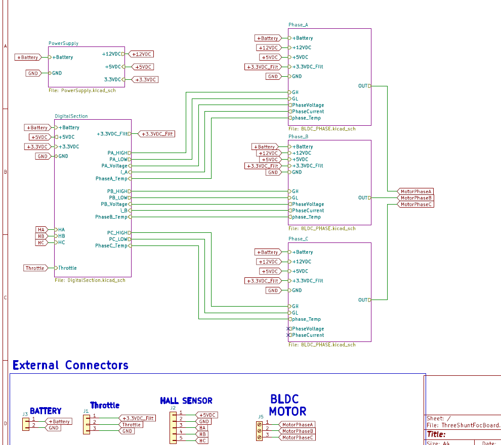
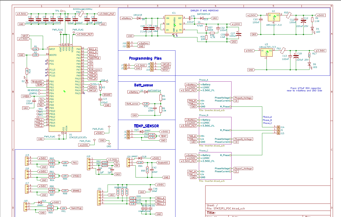
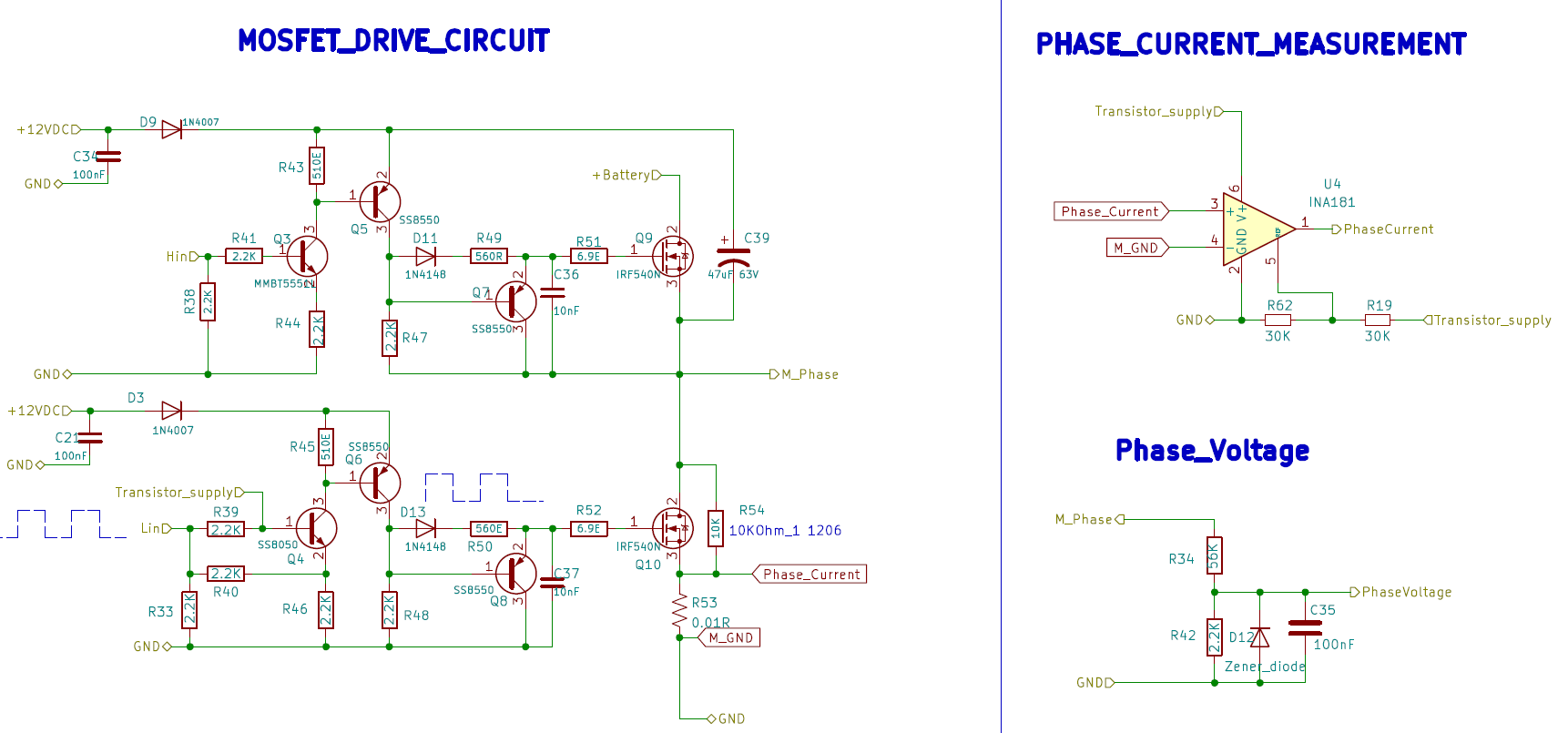
Based on this revised plan, I’ve designed a schematic using the STM32F103.
I’d be very grateful if you could take a look and share any suggestions or improvements you might have.
Thank you in advance for your time and support!
-BldcLover
Hello Everyone,
I’ve recently updated my schematic and would appreciate it if you could review it and share any suggestions or point out possible mistakes.
I’m currently in the process of selecting the MOSFETs, so that part is still pending. Due to budget constraints, I’m aiming to build a low-cost ESC.
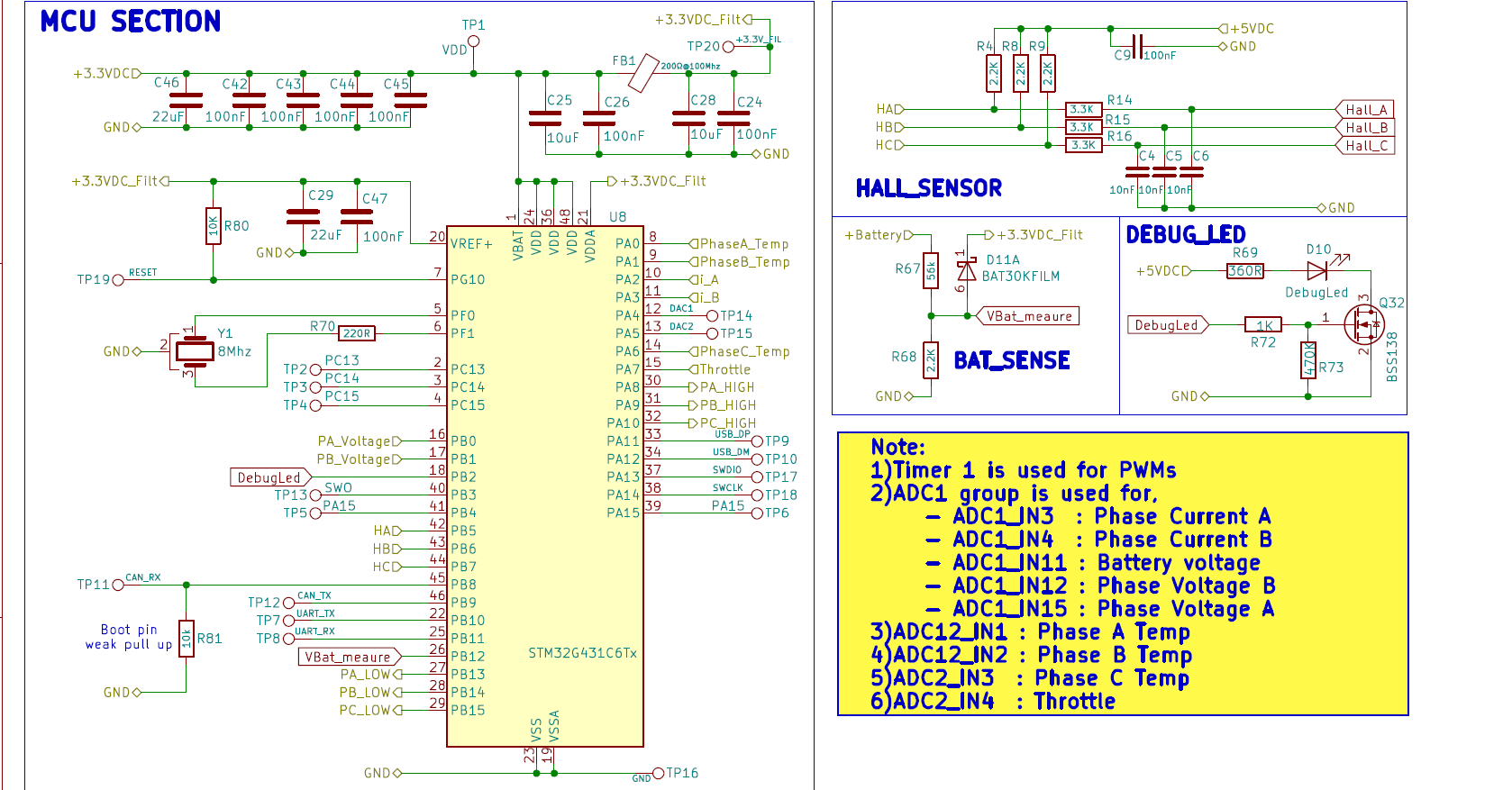
I’d also like to confirm whether the Hall sensor signals are correctly configured and functional in this design.
Thank you in advance for your time and support.
Best regards,
BldcLover
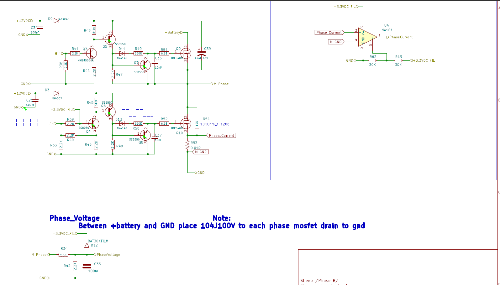
Additionally, I would like to know if transistors Q3 and Q4 will function correctly when driven with 3.3 VDC??
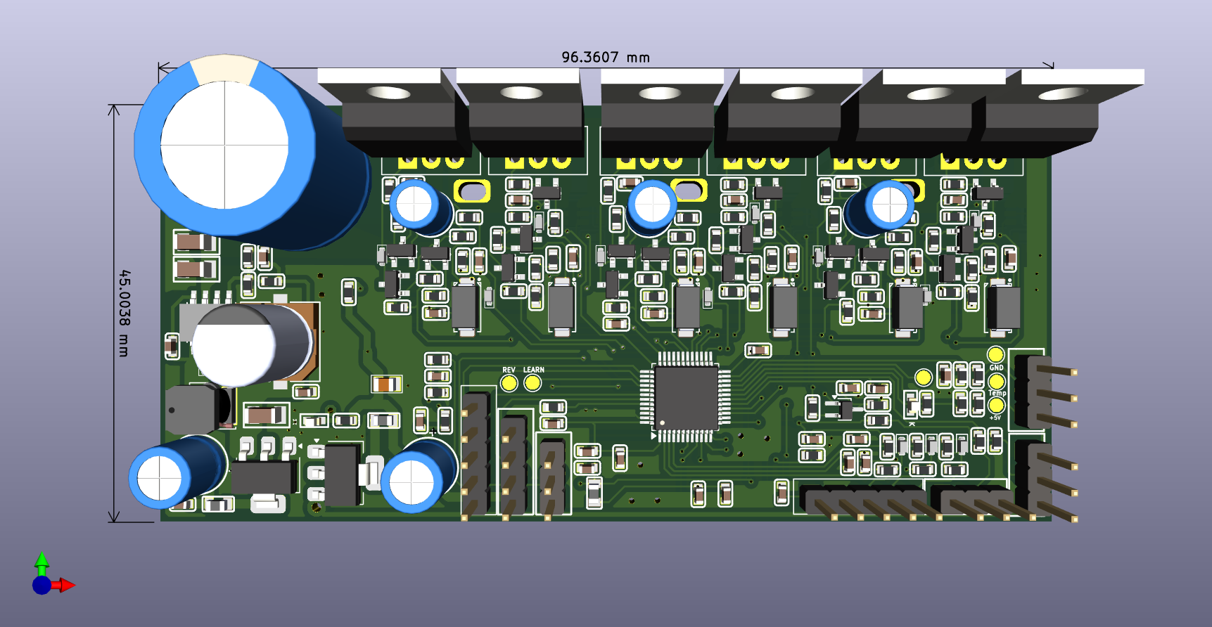
Hello everyone,
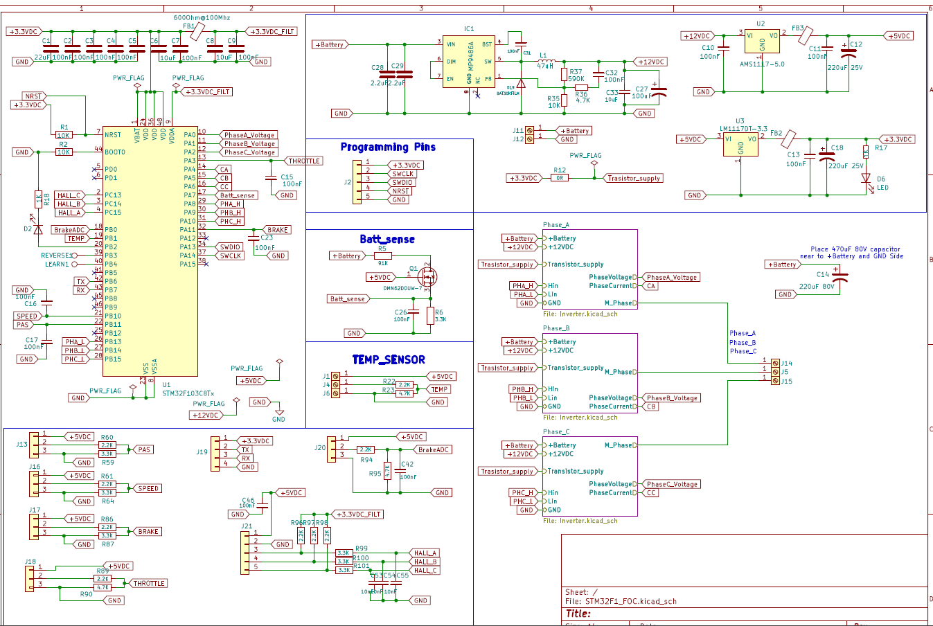
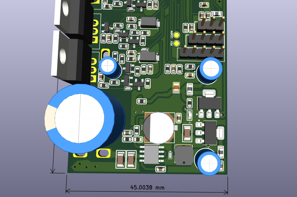
I have completed my design and now need to fine-tune some bottom layers, such as masking layers.
Please let me know if you have any suggestions or see any areas for improvement.
For Hall sensor detection, I have used the BAT30KFILM diode, the same one used in the B-G431B-ESC1 Discovery Kit.
Regarding the transistor logic: it is designed to operate at 3.3V and should work correctly at this level.
Best and regards,
BldcLover
![STM32F1_FOC_front_view|690x357]
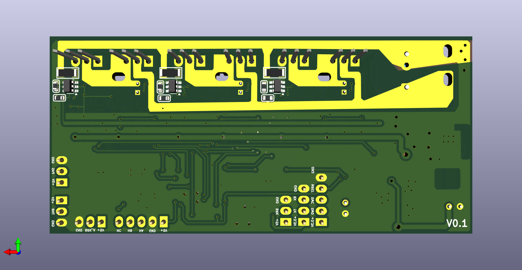
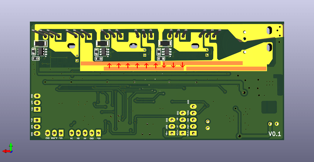
The power lines look too small. If you can move the bootstrap capacitors, you can make the traces going to the high side drain pins at least 3x as wide. See the leftmost one in the edited image (I filled over some vias too, but even if you have to cut into the copper area for them it will still be a major improvement).
Widen the ground traces to the sense resistors too. Then you can solder heavy copper wires along the main lines and probably have 3-4x your current current rating.
If you’re having the back side assembled by JLCPCB, you could use these little brass pieces that can be handled by pick-and-place machine: STHW4-DU-HS3001X510 | STEIPU | Price | In Stock | LCSC Electronics
But you’d need to widen the copper areas on the board to make good use of them. If you just put 2 or 3 of them end-to-end, there will be hotspots where the full current has to flow in the narrow PCB copper. It would be better to have two rows of them staggered so current can flow between them over a wide area of PCB copper (red arrows in the image). But you may have to widen the board a couple millimeters to fit them on the ground line.