First, I would like to introduce myself regarding this topic. I am a retired electrical engineer and specialist in EMC testing and design. In my work more years back I have designed smaller switch-mode power suplies and different high-power designs in 100 kW-range and 10 MVA range. I have not worked with ESC design, but I noticed more contributors here do it.
I have looked at some of the threads here and other places regarding using shunts to measure the current, and the problems included when you need to have a quite high measurement bandwidth. The self inductance of the shunt used is very important to consider in the design, and I have not noticed this issue to be addressed that much. When I look at the proposed PCB-designs from shunt manufacturers, then they only address the DC or low frequency aspects. This is why I am writing now. Please let me know, if you have seen this topic covered elsewhere.
I have seen previous threads here regarding this issue like here:
https://community.simplefoc.com/t/simplefoc-current-sensing-w-r-t-integrated-current-sensors-response-time/1018
But problems with current sense is discussed quite often.
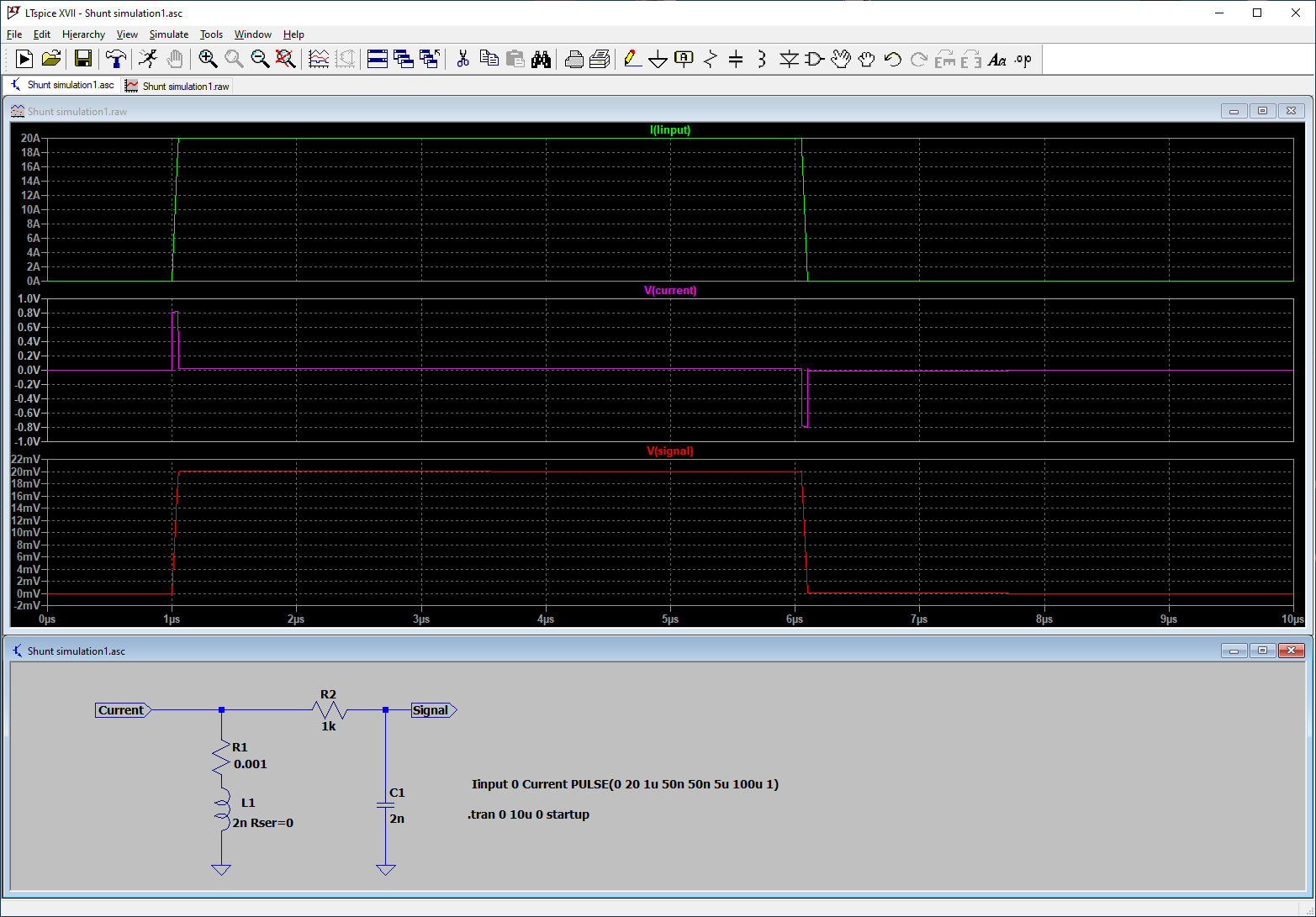
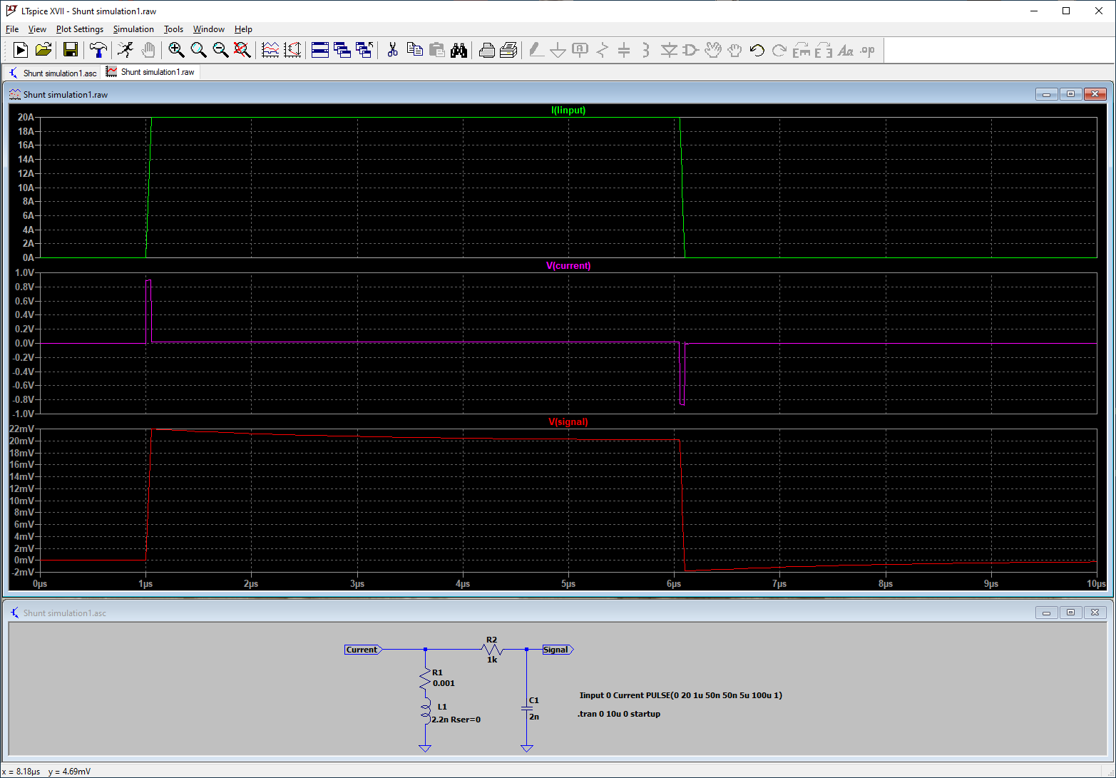
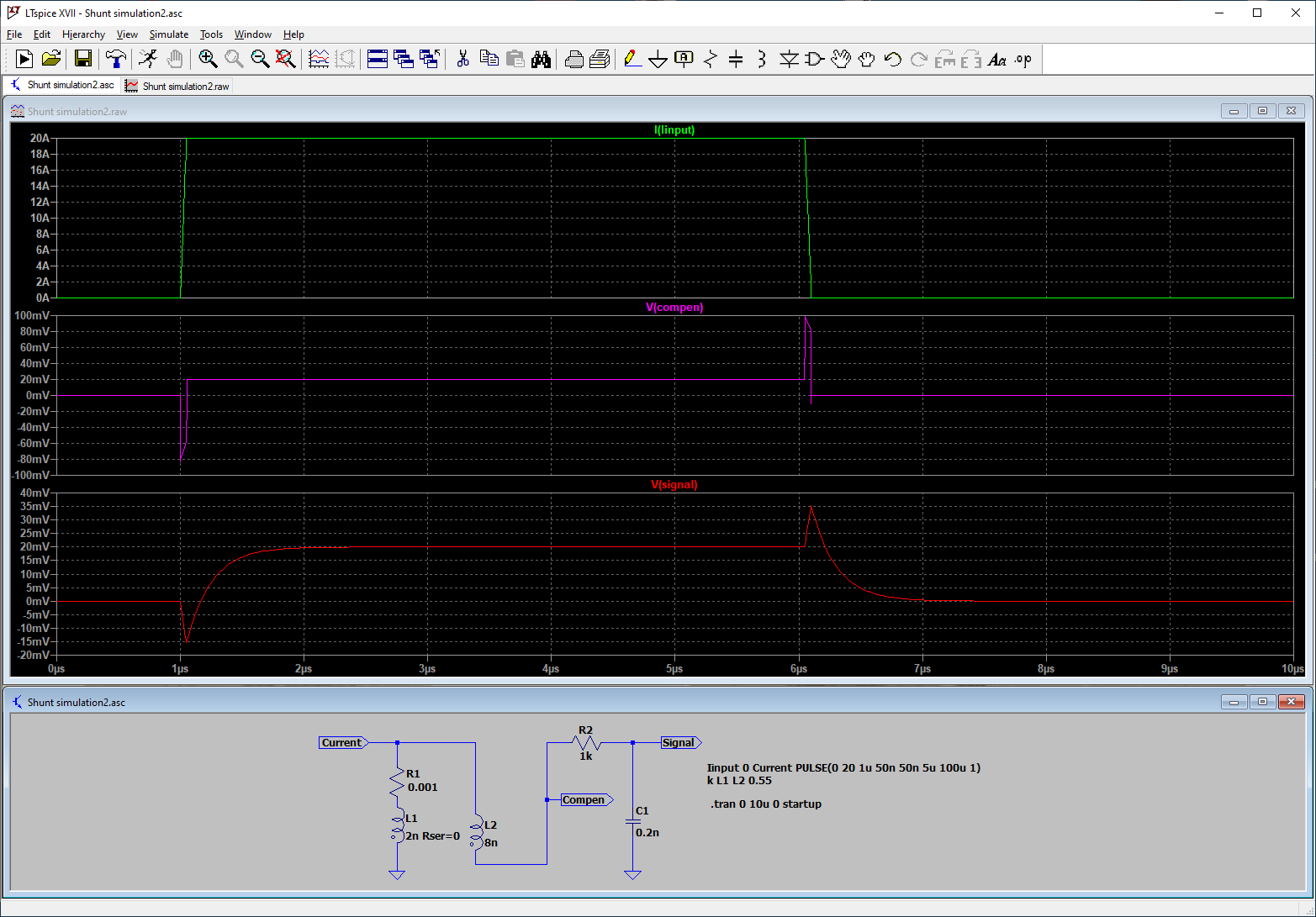
I use some simple simulations of shunt behavior and signal filtering in LTSpice to make some analysis. Consider a design with shunts connected to ground from the source of the lower mosfet transistors on the half bridges. In this proposal I use pulse current of 20 A and of 5 us in length and with 50 ns rise and fall times. The shunt used is a 1 mohm SMD resistor, and for this calculation I estimate a self inductance of 2 nH:

The transient voltage on the shunt is about 0.8 V and value to be measured is 20 mV. So if you use this signal directly to a signal amplifier, it is likely to saturate, and you get some will have to wait for the amplifier to recover. Then it is normal to make some RC low pass filtering of the signal, and in this case you got a time constant of 0.5 us or bandwidth of about 300 kHz.
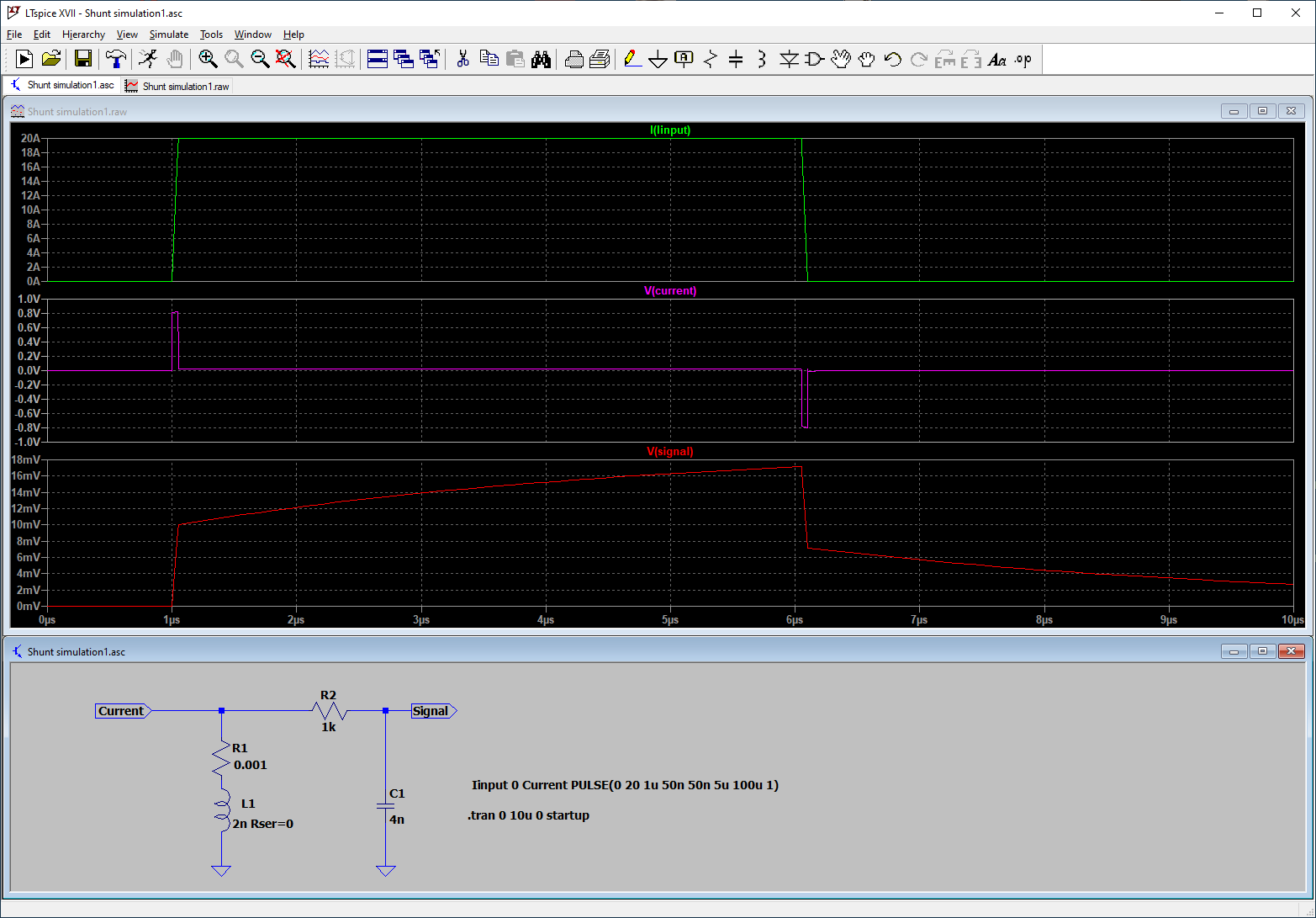
However, this is not an optimized design. You can optimize this by choosing an RC-filter with the same time constant as the time constant of the shunt (L/R). Then you actually get a perfect signal like this:
However, you need to be aware that you will have production inacuracies in actual self inductance and component values, and I do not expect that you can measure sensible before 2 us after a transition. But the aim here is to estimate the self inductance of the shunt and match the RC-filter afterwords.
This is how it looks like when you filter too much:
I this case you should wait about 5 us before you can measure reasonably.
Now, consider that you made the right RC compensation, but due to inaccuracies in shunt placement and PCB, the self inductance increased 10 % to 2.2 nH. Then you see this:
It will depend on how accurately you need to measure the current, how long you need to wait from after transition to when you sample the voltage in the ADC. I guess that with correct compensation you will need about 4 us for a resonable value.
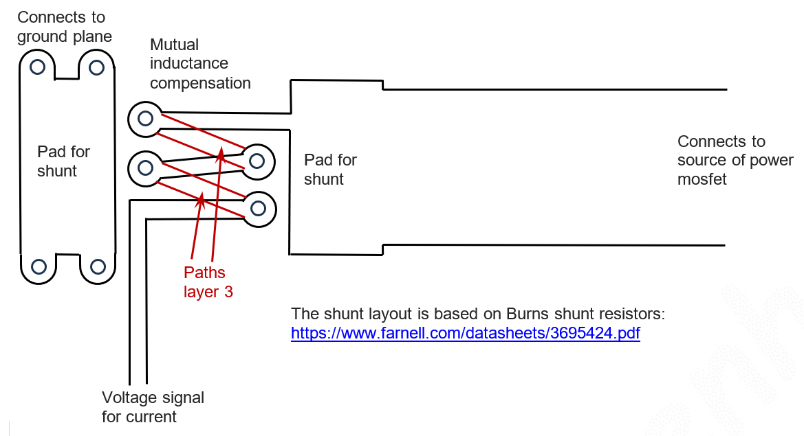
Another approch is to work with the PCB design and how mutual inductances can be utilized to make a better and faster current signal.
I consider a 4-layer PCB-layout with these principles:
Layer 1: Upper PCB layer with connections to shunt and Power mosfet
Layer 2: Gound plane layer with only through-hole penetrations
Layer 3: Layer with connections to many smaller connections (red marked)
Layer 4: Layer with large power connections
Or this layout:
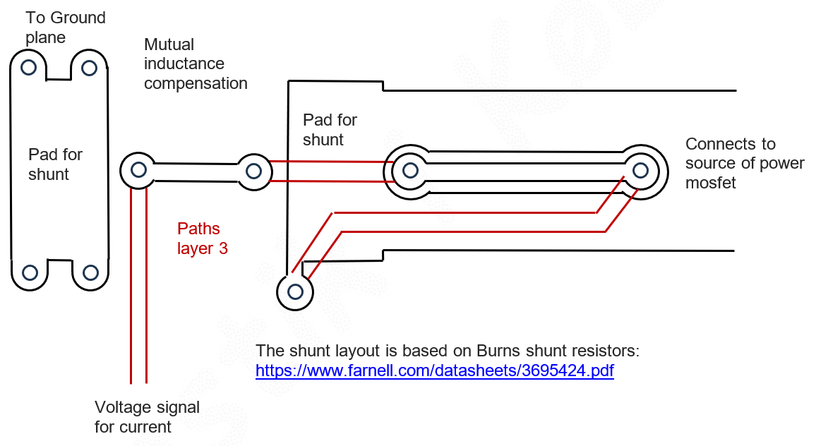
In these cases, the PCB design causes a mutual inductance to the signal, and it is the aim to eliminate the voltage caused by the self inductance of the shunt in the voltage signal from the shunt. For some SMD components it might be an issue to have through-hole plating below components so please consider a work around if this is the case.
These are the simulations of this case:

Here you see a situation, with slightly too little compensation. And the RC-filtering got a too high time constant for this.
This is a situation with the RC filter perfectly optimized for the same case:
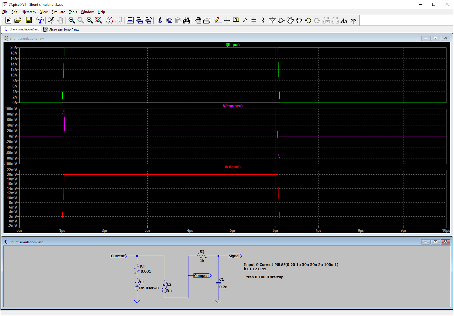
In the case below, the mutual inductance overcompensates a little:
I think, that if you both make a PCB design utilizing mutual inductance, and you make a matching RC-filter, you will eliminate possible saturation of the signal amplifier, and be able to measures the current signal within 1 us from the transition.
I hope this might be usefull for some of you.