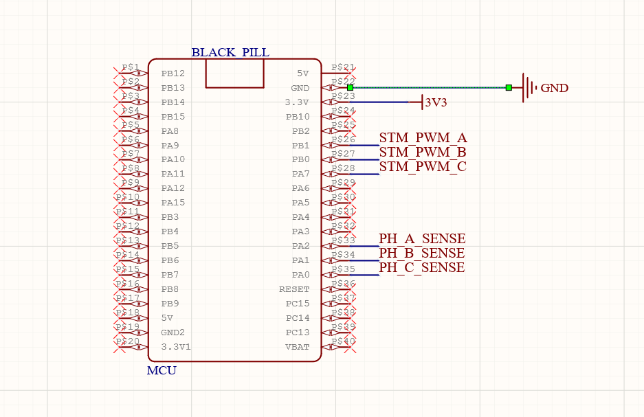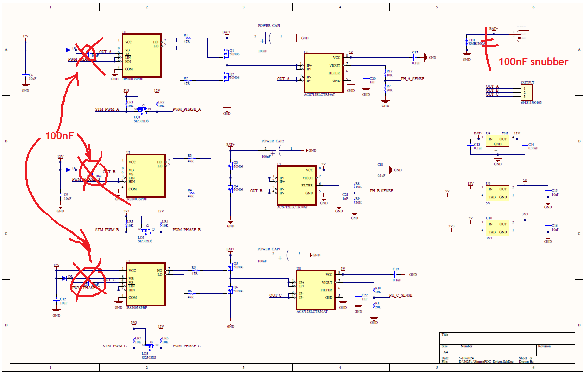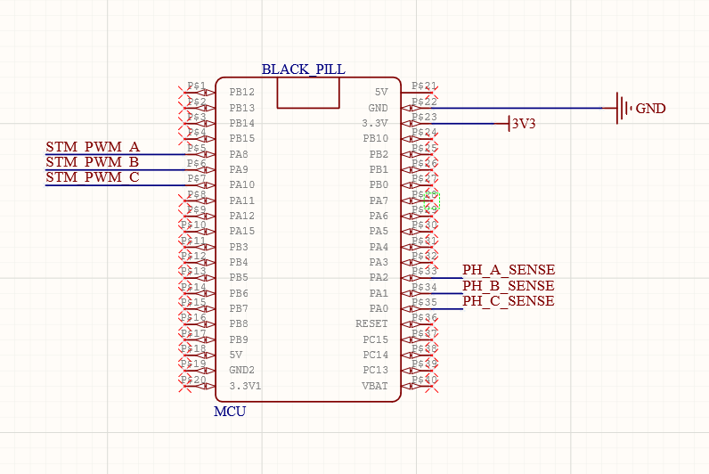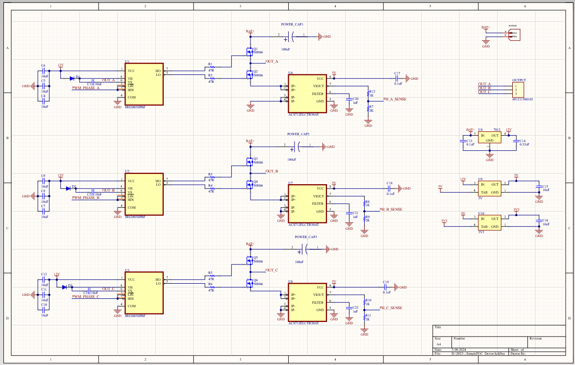
Implemented ACS712 in the existing design. Currently sticking to a voltage divider to translate the 5V adc to 3.3V.
Corrected the bootstrapping error.
Please review if I have missed anything. Routing this will be fun ![]()
Implemented ACS712 in the existing design. Currently sticking to a voltage divider to translate the 5V adc to 3.3V.
Corrected the bootstrapping error.
Please review if I have missed anything. Routing this will be fun ![]()
@Valentine @Andrew please help with the review.
Your resistor values for the voltage divider on the output of the ACS712 are too low, they should be increased so the total is at least 4.7kohm.
I suggest using a 10k and 20k resistor in place of your 1k and 2k resistor.
Other than that it looks fine
Interested to see the routing/layout.
Cheers,
Valentine
Lots of homework eh?
Cheers,
Valentine
Thanks Valentine, you’ve given me quite a bit of homework.
I’ll clarify my way of achieving my goal with some context. I have always struggled to foolproof closed loop mode with SimpleFOC before because of lack of proper hardware. My goal hence is to achieve that with maximum scalability (I should be able to source components and recreate the boards on demand without importing ICs).
I’ll do this in iterations, first being a POC only. Just to learn the “what not to do”.
Enhancements will be done once I have successfully spun my 5010 both sides.
Now, Before cleaning my mess, I want to confirm if the solutions I am thinking of are right. Please help me with that.
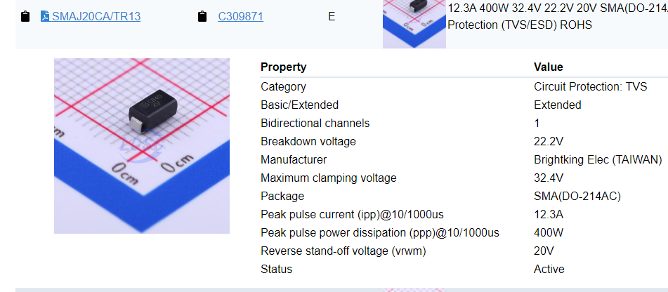
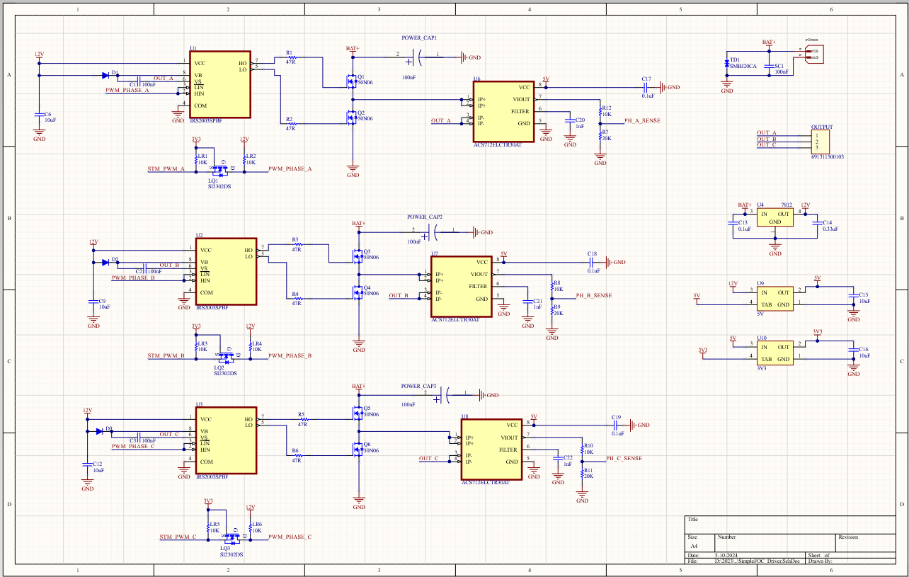
You need one TVS on the power input only. If you plan on 18V max, you need one TVS that breaks around 20V.
That’s 100nF boost cap equivalent. 1uF is too much. No need to change the mosfets. This is educational, not production grade board. If you don’t burn it, you havent learned.
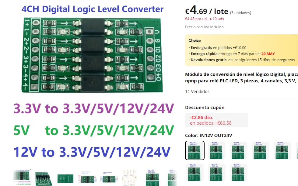
You can use an external voltage translator/shifter, as long as you know what are you doing. Don’t overcomplicate your circuit. Just buy it.
Cheers,
Valentine
SMBJ20CA TVS Diode seems to be right for this.
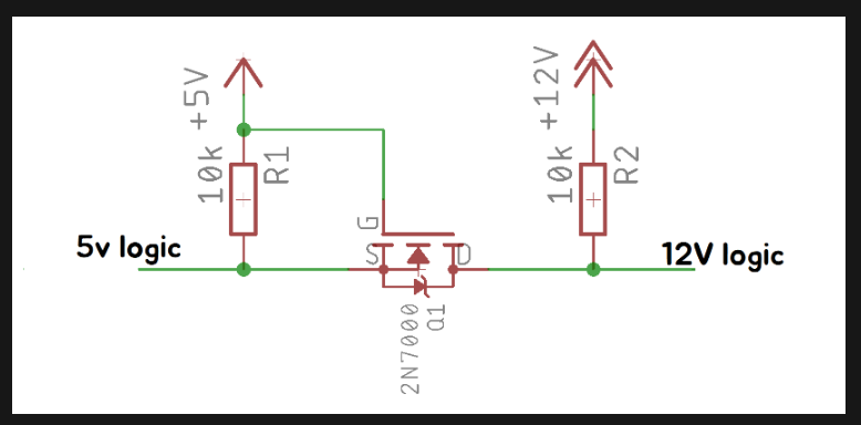
Soldering external modules will become messy, why not just implement a basic logic shifter like this?
Should be fine I guess. Cheers, Valentine
And im gonna keep trying until it is 100% correct ![]()
is it time to route yet? (Cant wait to do it)
Yes.
Cheers,
Valentine
Perhaps a stupid question.
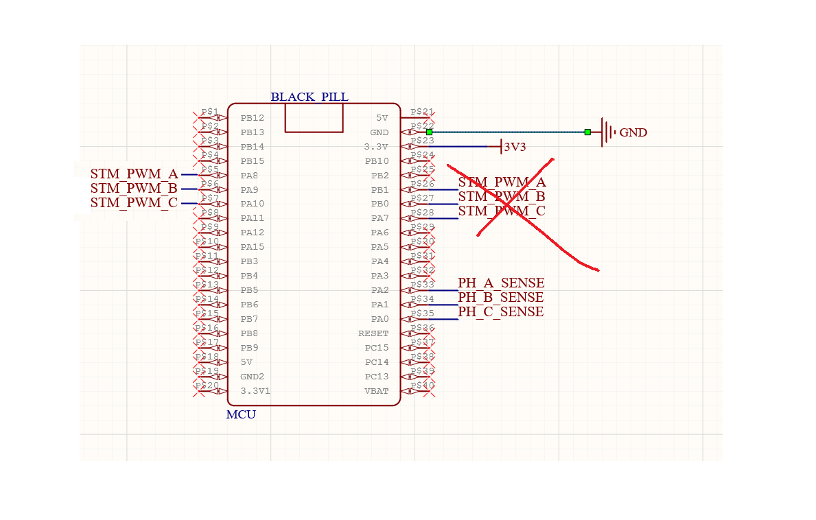
Why are you trying to go for 3PWM instead of 6PWM?
Cheers,
Valentine
To simplify things a bit, essentially 3 less probes to debug.
Also read this thread
IRS2003 supports 3 pwm setup, makes the schematic a tad bit less complex. (I’ve gone through the timing diagrams, while it does support 6pwm mode, Hi and Li_bar pins still can be used in negation to achieve the 3 pwm effect)
Am I missing something?
Not really. But 6pwm allows for more flexibility. You can always adapt later to 6pwm. Let’s table this topic. Focus on routing.
Cheers,
Valentine
Aye aye sir!
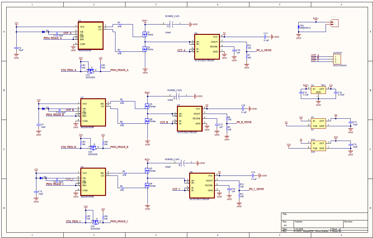
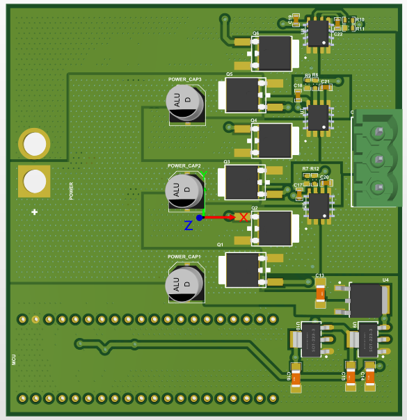
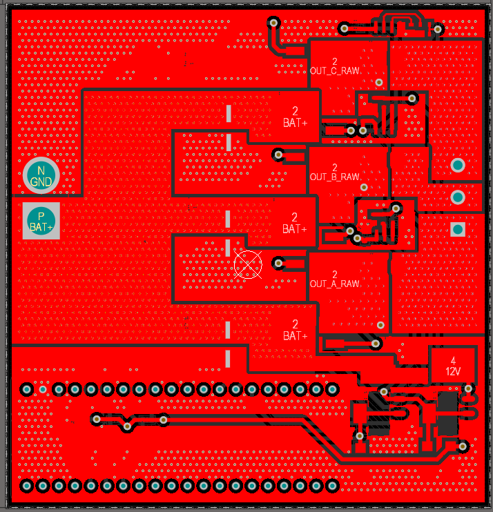
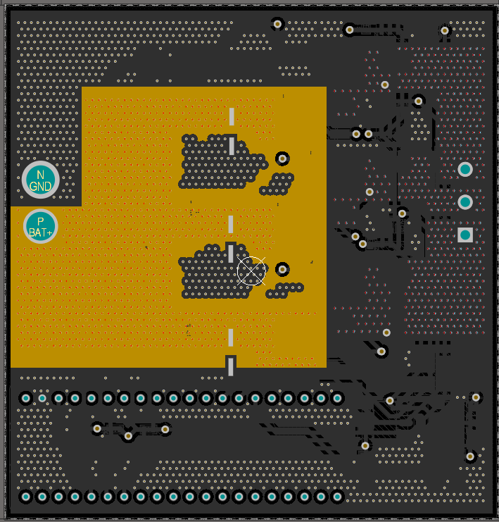
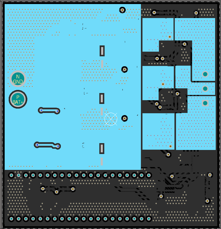
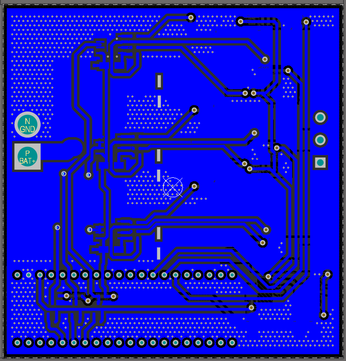
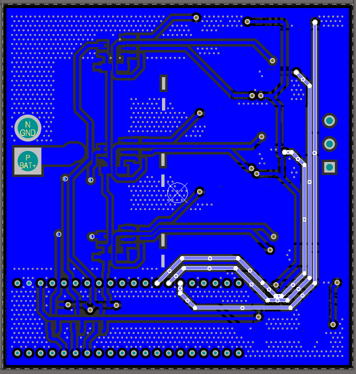
First iteration of routing :
4 Layers (POWER - POWER - GND - SIGNAL)
79.5 x 77 mm
Data via 50mil/30mil
Stitching via 0.5mm/0.3mm
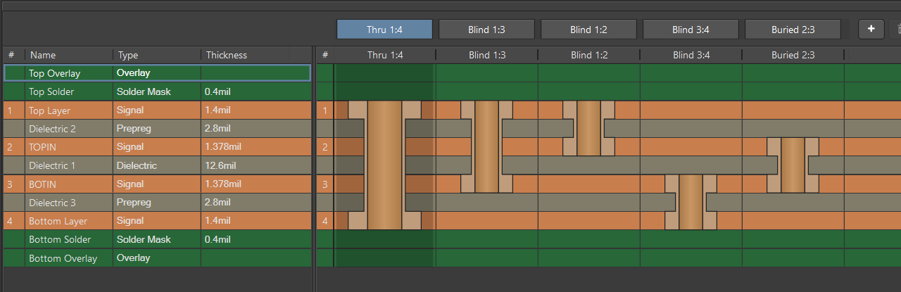
Layer stack and vias:
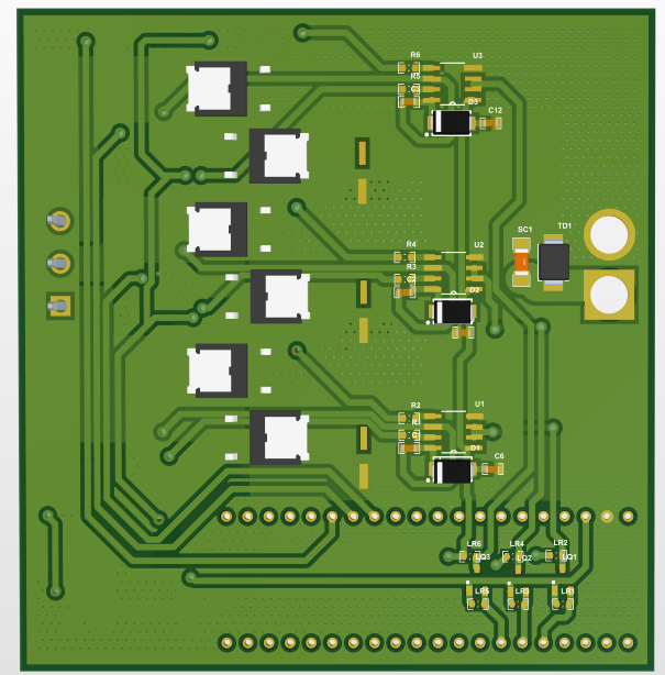
3D view :
Layers:
Top:
Inner Top:
Inner Bottom:
Current sense tracks:
Question, using Altium?
POWER - POWER - GND - SIGNAL
You are probably getting way ahead of the needs of the design. Don’t worry what’s what, just route it.
This is a mixed analog/digital so what you may have learned in school doesn’t really apply here.
If you really want to do it, you probably want
POWER/GND - SIGNAL/GND - SIGNAL/GND - POWER/GND
Let me check the rest.
Valentine
PS
I don’t see anything that stands out. It’s a little hard to gauge since it’s altium screenshots but it should work. One thing, you put way too many vias everywhere, you may want to think about placing them manually.
Do I see blind/buried vias? They are really cool, but for your design probably not necessary. Also they increase the cost of the PCB so much. I would really like to play around with those, but after seeing the $500 price tag on getting them manufactured my wallet couldn’t take it anymore and I had to limit myself to using only through holes.
I believe this is Altium standard way of showing the default layers, but yes, JLC don’t even make blind/buried vias. I didn’t see any in the design pictures but may be there are.
Using Altium for such projects is like shooting a mosquito with a cannon.
Cheers,
Valentine