-
Yes, I’m sponsored by Altium, I make all my designs in Altium.
-
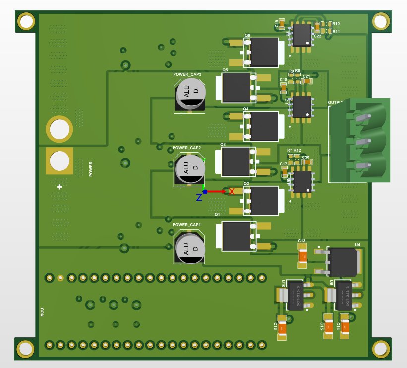
Regarding the layer stack, even if i state top layer to be “Power” it still has ground plane in it.
Everything is routed as is without giving any priority to “power” first. -
Yes, I will not be getting it PCBA ordered, I’ll solder everything myself. It’s a fun weekend activity for me, hence dual sided components.
-
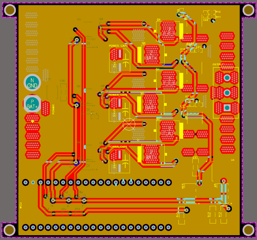
Stitching is generated by Altium automatically, while I can constrain the region of stitching, I don’t see any problem with extra stitching. Increases overall copper on the board.
The blind vias I saw were on BAT+ near the screw terminal. There’s a whole patch of them.
Using Altium for such projects is a good way to get experience with the software and it might help you get a job easier, as many companies are using Altium and not KiCad or EasyEDA.
Using Altium might even have some other benefits as well, such as the ability to do thermal analysis of the boards. It’s probably worth using for my new motor driver using RDS(on) current sensing, but I ended up just doing the thermal calculations by hand (ended up with max 20degc difference between temp sensor and MOSFET junction temp).
I’ve used Altium for some university projects in the past, and I can say once you get used to the interface it should be just as good as any other software.
Jlcpcb once printed by board of burried vias without any extra cost. Also, I’m getting these boards printed from a local vendor, who provides blind/burried vias without any extra cost.
PS I am not a beginner in PCB designing, I’ve been doing it for 6 years now. To Altium or not To Altium is not in scope because like I mentioned, I’m sponsored by Altium. it’s tools are now in my muscle memory, also I personally do not like any other softwares.
Hello Andrew and Valentine,
-
Now Switching to a Power/Gnd - Signal - Signal - Power/Gnd stack, without burried vias.
-
Will try to add stitching manually this time to avoid huge amount of vias.
-
Will add M3 mounting holes at all corners
I will share the next iteration of routing soon.
Thanks
Which vendor is that? Do they also SMD?
Cheers,
Valentine
It’s called robu.in , the warehouse of it is in same city that I live in. Hence I get a lovely 1 day delivery for components.
I doubt if it ships internationally. My last order of blind/burried vias from them for a 4 Layer board 100*100mm was Rs.1600, which is about $20
I’ve had a look at the robu.in website, and I think what they do is just forward your orders to JLCPCB and then ship them back to you. They might be combining shipping with other customers orders to save costs, due to their long lead times. I am assuming this is what is happening as most of the text on their PCB order page is copied and pasted straight from JLCPCB. (https://robu.in/product/online-pcb-manufacturing-service/)
Their website also clearly states they don’t support blind/buried vias, the page is also copied and pasted straight from JLCPCB, although it’s an older version of JLCPCB capabilities. (https://robu.in/pcb-manufacturing-capabilities)
I highly doubt they are able to produce blind/buried vias, but just to confirm, are you able to send a photo of your previous board, circling the location of the blind via on both sides? You should see the via on one side of the board but not the other. Unfortunately if your board only used buried vias it will be harder to verify, but you can try testing for continuity with a multimeter.
I suspect your blind/buried vias were either converted to through holes, or they were not manufactured at all. JLCPCB sometimes messes with your files before production, so they could have moved some of your other traces around to make room to convert the blind/buried vias into a through hole. You can choose the confirm production file option if you want to check what they did and reject the changes if unsatisfied.
Please report back with your findings, I am very interested to get to the bottom of this story.


Most probably the case. The vias are plugged by default so you can’t tell if it was a through via or not to begin with.
Valentine
I cannot see any big issues.
Cheers,
Valentine
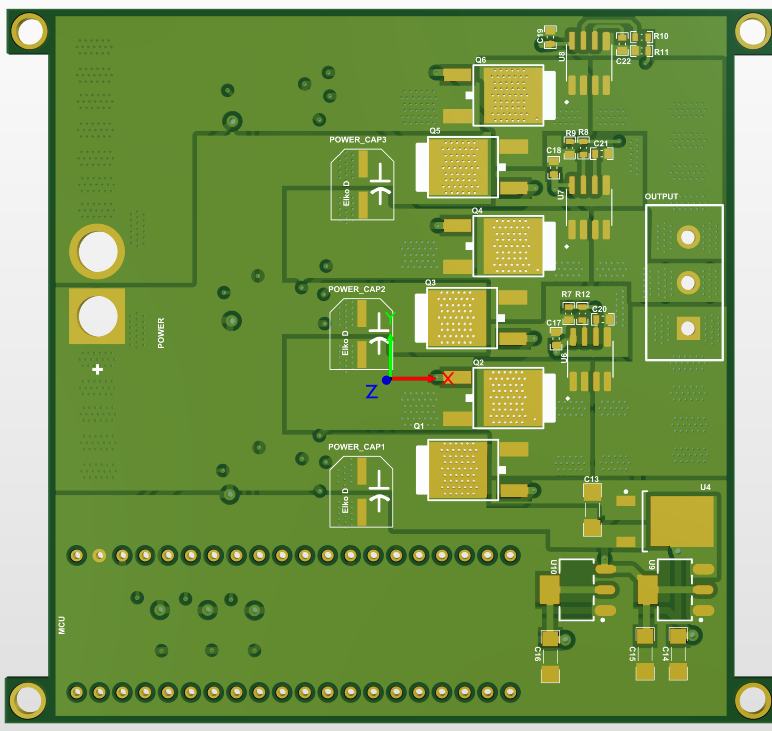
Mostly looks good, except a few minor things
The traces near POWER_CAP_1 don’t look very nice, but it will still work fine.
The output trace of phase B has a bit of a bottleneck, but it’s not a major issue.
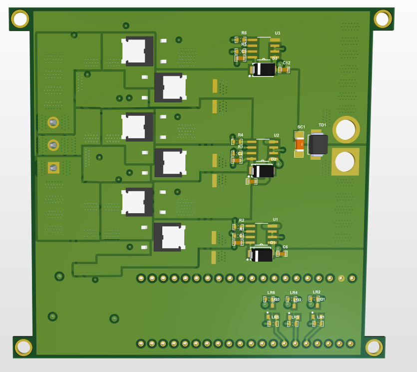
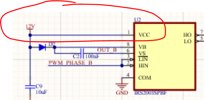
Are you sure the level shifters are necessary, as the datasheet of the IRS2003 suggests the logic inputs are directly compatible with 3.3V logic?
The disadvantage of leaving them in is that they will slow down the edges of the PWM slightly, and increase power comsumption.
He (she?) is not feeding 3v3 to Vcc so yes he heeds them.
![]()
That driver is really, really basic, the driver power and logic power are tied to the same pin/voltage.
The documentation is very confusing, yes, not clear what they meant unless you read everything very carefully. In fact even if you read everything you will be left with the impression it would work. There was a similar case with my Krakatoa board, the person tried and ended up mailing me the board to find out he was pushing 12V vcc and 3v pwm. The output was hi-z. Go figure.
Cheers,
Valentine
You’ve taken the screenshot from the absulute maximum ratings, which specify what range the voltages need to be within for the device to not blow up. The correct rating can be found further down:
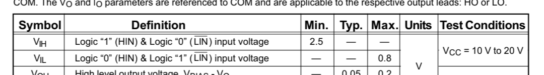
It says the driver will recognise any voltage above 2.5V as logic 1 for HIN or logic 0 for LIN. So since 3.3V is above 2.5V by a sufficient margin, no level shifters are needed.
Unless the datasheet is wrong and they haven’t fixed it, I don’t think the logic levels were the cause of the issue on your previous board. (Previously I found some errors in the DRV8316 datasheet, I contacted TI and they said they would revise the next revision and fix it)
Sadly they were so here we are. He can try both ways, may be he will get lucky. This is an educational exercise.
Cheers,
Valentine
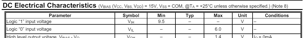
I’ve had a look at your KRAKATOA board, and I can confirm it won’t work with 3.3V logic because you didn’t pick 3.3V compatible chips. I’ve attached a screenshot from the datasheet of your driver chip (DGD2110) which shows this:
So it should be safe to remove the level shifters in this design as the datasheet of the chip confirms it is 3.3V logic compatible, unless you do not trust Infineon to provide correct information in their datasheets.
Okay,
One solution could be to add a solderable jumper to bypass the level shifter.
This way I can test both signals, sifted one and raw one to check if it works either ways.
I’ll add that and send the board to manufacturing.

I think you’ve resigned it by now, but to comment on the blind/buried vias issue: you have to consider how the board can be manufactured. Vias have to drilled into the stackup, one way or another, and the factory has to be able to do it within the processes they know how to do…
So for example the first via type is through board, and would be drilled through at the end in basically any process I think. The 3 via types on the right are blind/buried, and could (for example) be made in a HDI 1+2+1 process with an inner core with two copper layers and one layer added to each side, and the vias drilled as mechanical or laser microvias. The via type 2 would probably be realised as “stacked microvias”.
All of this will be hugely expensive, and outside of any kind of “pooled process” they can offer - they’ll be running the machines on a full sized factory board that’s just for you, whatever the size of your design, and you’ll be paying for that full size and all the process steps used…
Anyways, it sounds like you’ve fixed it, so I’ll be very interested to hear about your results!