Request for Comment: Dual DRV8316 SPI 3PWM Driver

Hello Everyone,

I am working on a robotics project that require control of two BLDC motors with stator size about 2208. I need a solution that is as flexible as possible to experiment with different designs. I have been following great development projects based on the TI DRV8316 Three-Phase Integrated FET Motor Driver.

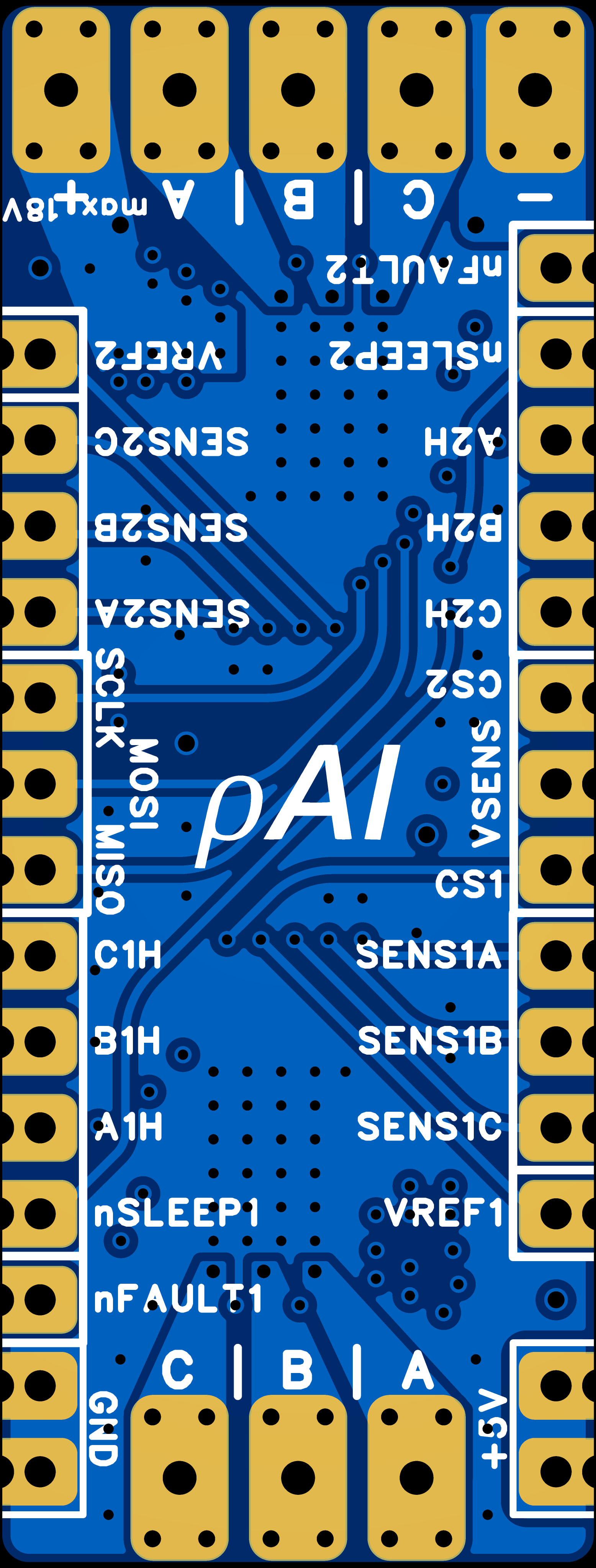
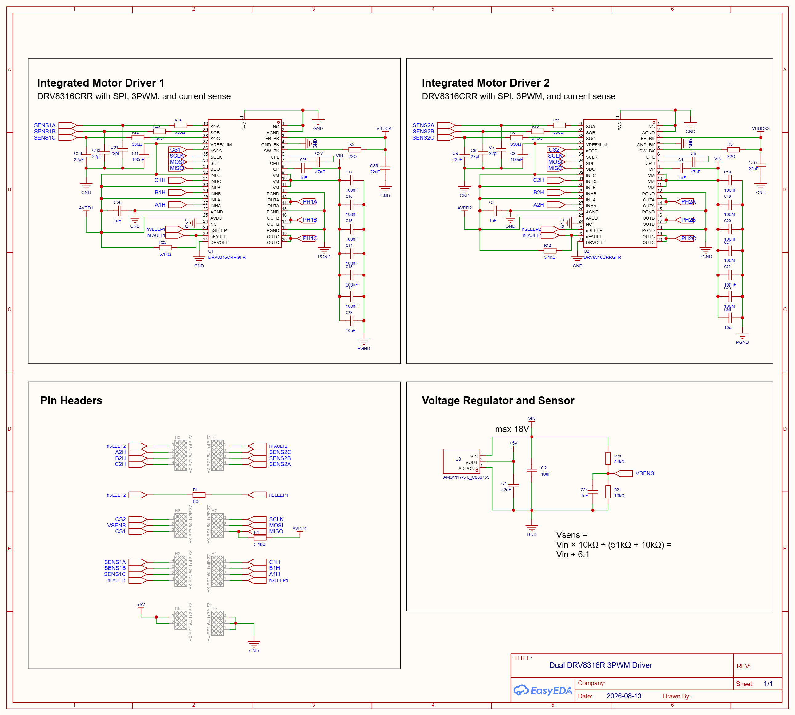
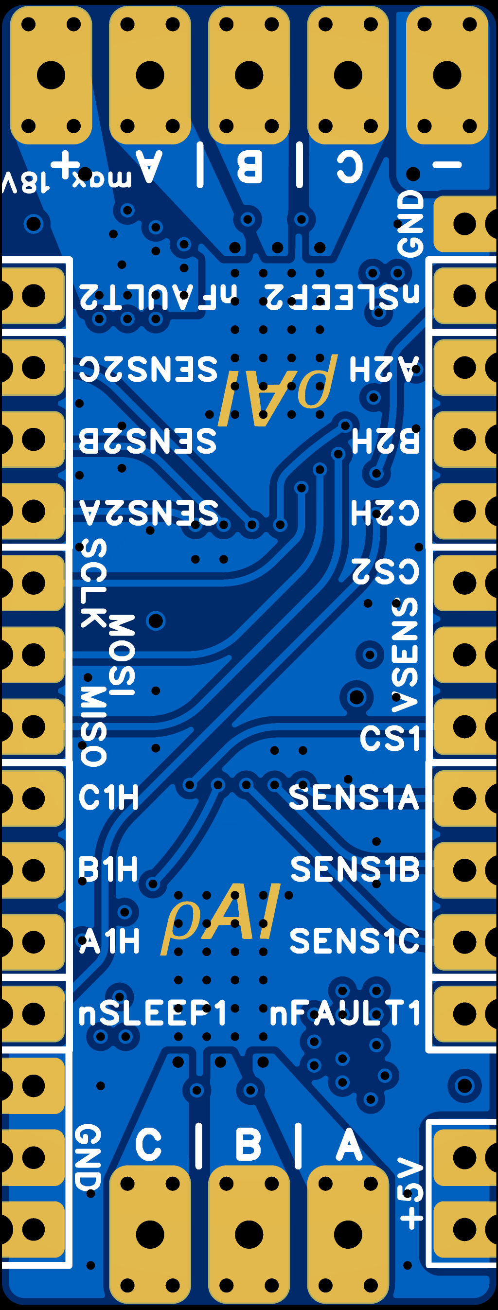
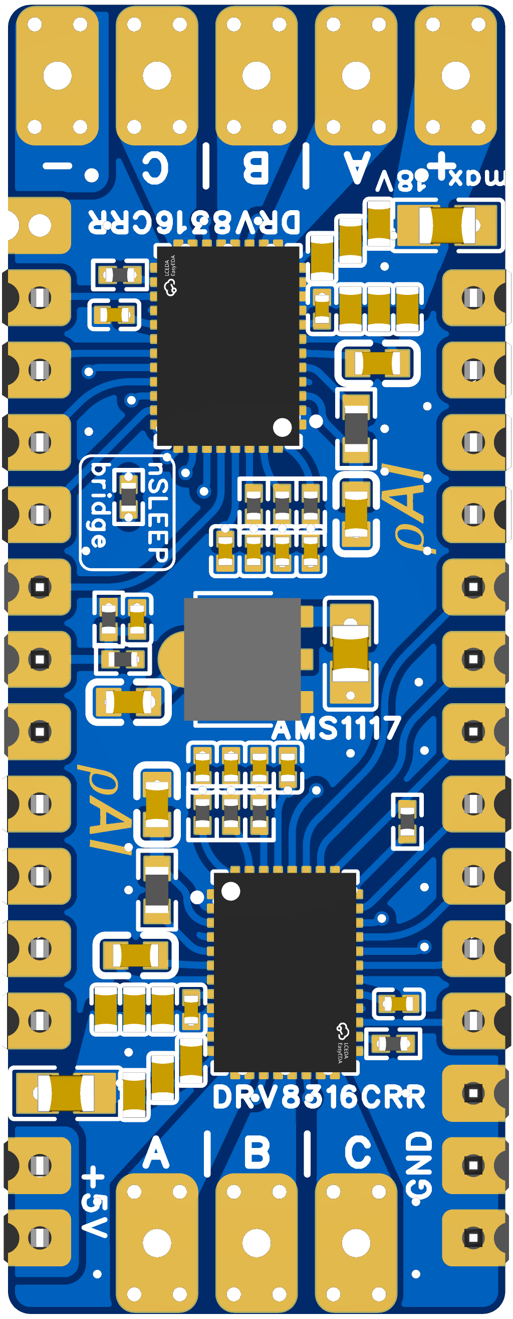
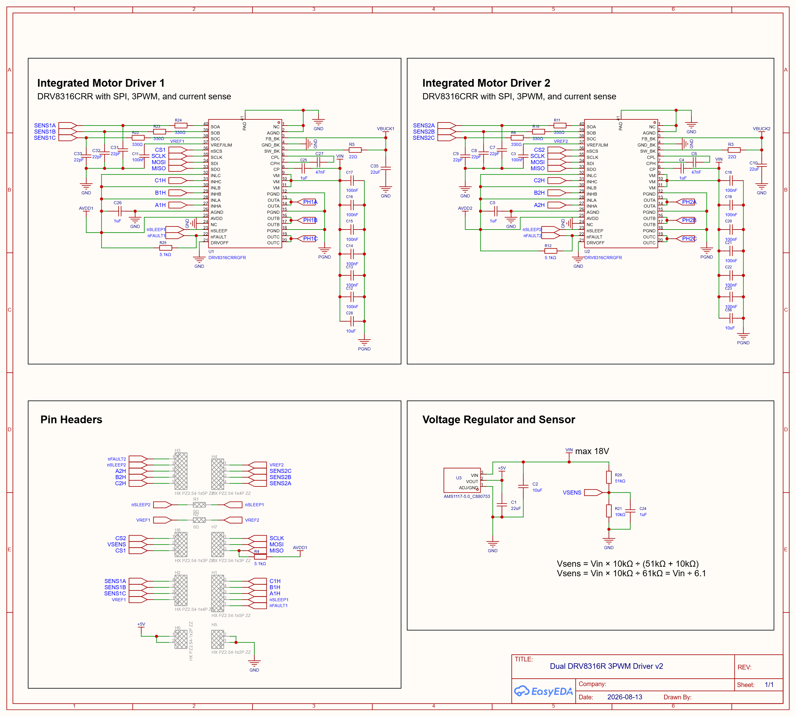
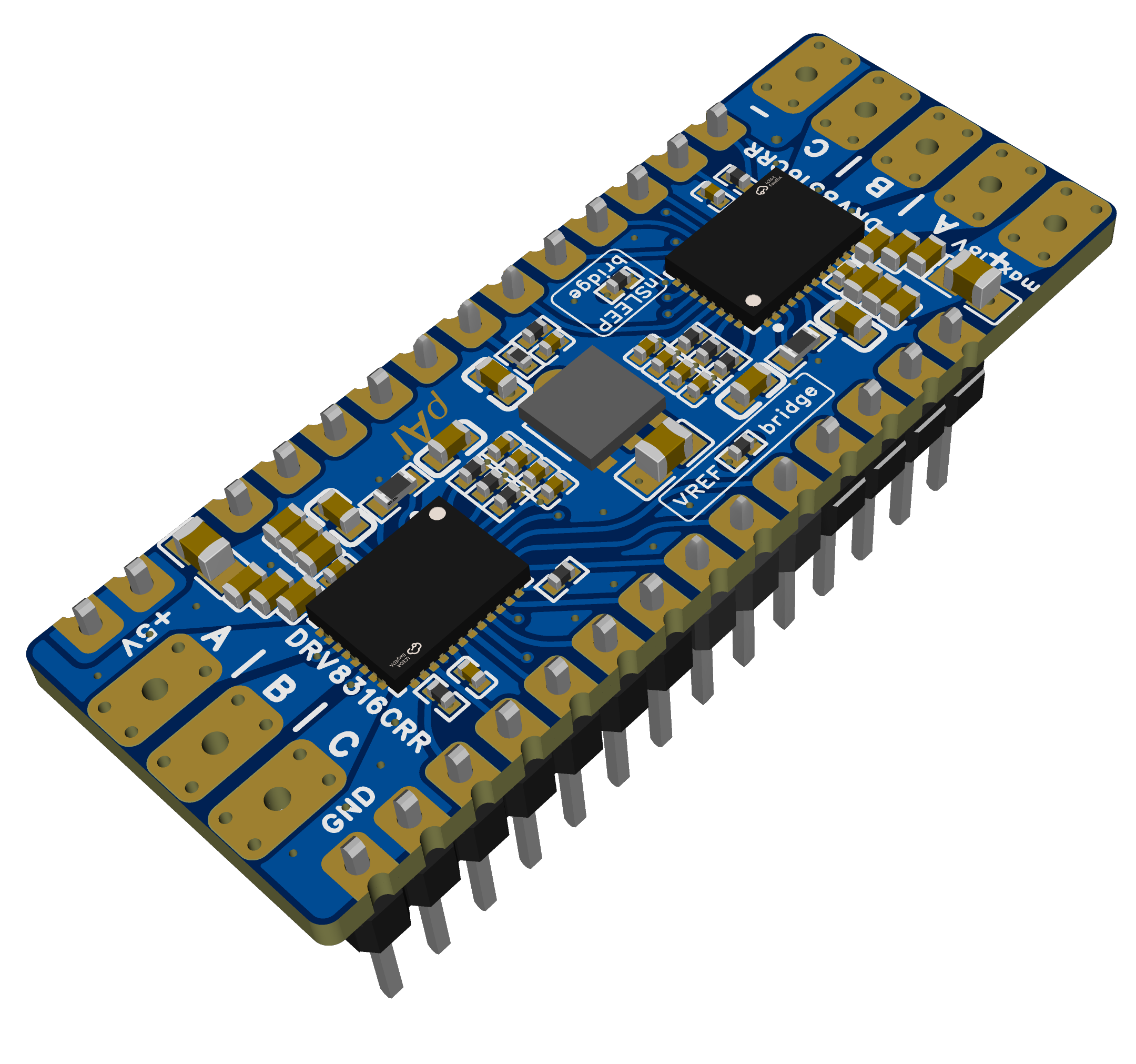
I designed a driver board based on two DRV8316 drivers and an AMS1117-5V voltage regulator. I adhered strictly with the datasheets for selection of each component. This board can be paired with any MCU board through a carrier board. The MCU would be mounted on one side of the carrier; this driver board would be mounted on the other side. This solution allows me to try different MCUs without redesigning and ordering a different batch of boards. The carrier board is simple enough that I can cut as a single layer on a SainSmart desktop CNC machine.

If anyone in this community has some time, please take a look at the schematics and add some comments.

Features of this driver board:

  • 6-layers: Internal1 = GND; Internal2 = PowerGND; Internal3 = VIN; Internal4 = GND
  • Shared SPI port with separate Chip Select pins for configuring each DRV8316
  • 5V 1A voltage regulator output for powering an external MCU
  • Voltage sense output that measures Power Input Voltage (Vin = Vsens × 6.1)
  • Removeable 0Ω bridge for nSLEEP wires from both drivers to share a single MCU pin
  • Removeable 0Ω bridge for VREF wires from both drivers to share a single voltage input
  • VREF can be externally tied to 3.3V if DRV8316 is configured for mode 1 or mode 3.
  • VREF can be connected to a voltage divider or a DAC pin that provides 1.25V - 1.65V input if DRV8316 is configured for mode 2 or mode 4. This voltage input sets the internal threshold for cycle-by-cycle current limit modes.
  • Power Input and Motor Outputs can be soldered directly or connected with 3.5mm Pitch Terminal Block Connectors.
  • Space enough for mounting header pins on top side or bottom of driver board. This allows changing of driver board orientation relative to the MCU board. This may be necessary to align the current sense output pins SENSxx on the driver board with the ADC pins on the MCU.

Minimal requirements of the MCU or processor module:

  • 1 SPI port, preferably dedicated to the drivers
  • 2 PWM channels x 3 pins each channel
  • 2 ADC channels x 3 pins each channel
  • 1 ADC pin if Vsense (Power Input Voltage Sense) is required
  • 5 - 6 digital IO pins, depending on configuration
  • 1 - 2 DAC pins for VREF in mode 2 and mode 4, see VREF options above

It seems the ESP32-S3 has the required number of SPI ports, ADC channels, and PWM channels. All GPIO pins are configurable in software. This kind of flexibility makes this MCU an ideal fit for this driver board. Please let me know if there is a better MCU for me to try with SimpleFOC.
9 Answers

9

I decided to hardwire VREF pins to 3.3V because current sense outputs (SOx) on the DRV8316 are not available for PWM modes 2 and 4. I will share this design on oshwlab after I get some confirmation or comments for correction.

All other features remain the same:

  • 6-layers: Top - GND - Power GND - VIN - GND - Bottom
  • Shared SPI port with separate Chip Select pins for each DRV8316
  • 5V 1A voltage regulator output for powering an external MCU
  • Power Input voltage sense output (Vin = Vsens × 6.1)
  • Removeable 0Ω bridge for both nSLEEP wires to share a single MCU pin

I managed to find your design on OSHWLab. It’s better to post the link as it’s much easier to review live schematics rather than going off screenshots which are missing a lot of information.

There seems to be no connection between the GND and PGND nets. Be aware the datasheet mentions that the maximum voltage difference between the different kinds of GND pins is 0.3V, it’s really easy for a user to accidentally violate this with edge cases in power sequencing. It’s recommended to not use split grounds unless you have a good reason for it, as usually it causes more problems than it solves.

Also there is not enough capacitance on board, which would cause very large voltage ripple if the wiring is long and has high inductance, and the board is being run at high current. For this board I would recommend at least 200uF of capacitance, and probably the sweet spot is around 600uF. You should use polymer or electrolytic capacitors for this as ceramic capacitors lose capacitance quickly when voltage is applied. Keep the ceramics you have now as they are better at handling the high frequencies.

Although the datasheet only shows a 100nF + 10uF capacitor, if you look at the images of the DRV8316REVM you can see they used a 330uF capacitor.

The ESP32-S3 could draw up to 400mA when wifi is transmitting. Even if we assume an average draw of 100mA, the power dissipation in the LDO would be (18V-5V)*0.1A=1.3W and this exceeds the absolute maximum ratings of the AMS1117 you picked (500mW max power dissipation in SOT89). One other thing is that the AMS1117 you picked is rated for 18V but most other AMS1117 on the market are only rated for 15V, this is not an issue with your design, but it is something to be aware of when ordering to not accidentally substitute the part.

The buck converters of the DRV8316 might not be sufficient for the ESP32-S3 since they are only good to 200mA while the ESP32-S3 sould draw 400mA, and you shouldn’t put the 2 bucks in parallel because it’s not guaranteed they will share current evenly.

So for your application you might need to resort to a discrete buck converter, such as the TPS54302. Alternatively you can limit the board to only using lower power draw MCUs and use one of the integrated buck converters from the DRV8316.

The STM32G4 series is usually the first choice for motor control, as the feature set aligns very well with motor control applications.

Finally, you can also have a look at my previous motor driver designs for more guidance.

Thank you @Andrew for your very thorough analysis. I need some more advice. I looked at various designs on oshwlab and this board. I followed guidelines of the the datasheet (https://www.ti.com/lit/ds/symlink/drv8316.pdf); but I do not understand a lot of it.

  • I saw this part in section 11.1 Layout Guidelines, “To reduce noise coupling and EMI interference from large transient currents into small-current signal paths, grounding should be partitioned between PGND and AGND.” Somehow I missed the last part of that paragraph about “Ensure grounds are connected through net-ties or wide resistors to reduce voltage offsets and maintain gate driver performance.” Is it be better to use separate ground planes connected through net-ties? Or is it better to accept some level of EMI interference by using one common ground?
  • In Table 6.1 row on VM, “bypass to PGND with two 0.1-µF capacitors (for each pin) plus one bulk capacitor rated for VM.” I saw different designs use different quantity and values for bypass capacitors without any explanation. The Microspora board use 5x 10uF. The SimpleFOCMini V2 use 100nF + 10uF. Your BLDC driver v4 design use 100nF + 10uF + 4x 22uF and 2x 330uF. That is a lot more than datasheet guidelines or any previous designs. I am still very confused about appropriate quantity and values to use for bulk capacitance. This is intended for a robotics project where two 2208 motors are not expected to run any faster than 1800rpm. I can follow your design for local capacitance 100nF + 10uF + 4x 22uF. What can I use for bulk capacitance in a smaller package than a 10x10mm can?
  • I understand the tradeoff when using a smaller package for the AMS1117-5V LDO. Thank you for providing the numbers in your explanation. I will use a larger package for better heat dissipation and add a heatsink on each chip.
  • The buck converter output from both drivers are not output to any pin headers for use off-board. They are not used to drive any pins on-board. The only voltage regulator output is the 5V from the AMS1117-5V LDO.

Thank you very much again for your help.

Ted N.

It’s better to use one common ground and mitigate the noise coupling another way. The easiest way is to make sure your ground planes are wide and don’t have too many bottlenecks, this mitigates the low frequency noise caused by the high current, and you have good decoupling and bulk capacitance, so any high freuqency interference is suppressed by the capacitors.

No it’s not necessary to follow the capacitance values exactly. Going bigger than recommendation in the datasheet usually doesn’t cause any issues. It is important to place the capacitors as close as possible to the power and ground pins, the exact value used is less important, but bigger capacitors are harder to place physically. The v4 design is old and designed with hand assembly in mind, so I would say the choice of capacitance there is not optimal, because it would be possible to cram a larger ceramic like 10uF closer to the power and GND pins if machine assembly was used.

For your design, my recommendation is to put 2x 10uF close to the VM and GND pins of each DRV8316, plus 200uF of bulk capacitance anywhere on the same PCB. If you want something smaller than electrolytics, you can use tantalum polymers but they are a lot more expensive, see my v5 and v6 designs which use these.

The amount of capacitance needed is determined the maximum current you will be running and the pwm frequency, rather than the motor size or motor rpm. I am assuming here you will be running at 8A per motor and with 50KHz PWM, let me know if you plan to run it differently.

The amount of capacitance chosen is calculated to have the ripple voltage being less than 0.5V given the source inductance is large. The amps used in the formula below is half the motor current amps (you have 16A total since 2 motors), and the time is half the PWM period, to do a rough estimate of the ripple voltage across the capacitor. Note the formula neglects the capacitor ESR. Of course if you think 0.4V is too high then you need to increase the capacitance. Usually for my designs I aim for less than 0.2V.
(8A*10us)/200 uF=0.4V

You can also look at the Gooser series from dekutree64 on the forum or here: Gooser5.8 - Platform for creating and sharing projects - OSHWLab
This board is using discrete MOSFETs and has a good amount of capacitance.

The recommendation here is not to use a bigger package for the LDO rather it’s much better to replace it with a buck converter due to the large voltage difference between the input and output. The integrated buck converter suggestion is to save costs compared to using a discrete one, though the disadvantage is the lower current and 3.3V by default behaviour, though this is fine for most MCUs which run off 3.3v natively. Your board size is already very small so total heat dissipation is a concern here.

Thank you! That is unbelievably simple. I’ve just been blindly following Valentine’s edict for 1000uF on Lepton many years ago, assuming that it could only be determined by complicated simulations or something. For Gooser’s 30A max and 25KHz PWM, 15A*20µs/1000uF = 0.3V. And minimum is 600uF. I had considered making a minimal size single motor 12V version with 11x47uF 25V rated ceramics, and now I can finally see that it would be able to do 25A or a bit less since there will still be some DC bias effect despite the voltage being over 50% derated already. Not bad.

I agree on combining the PGND and AGND nets. Everything I’ve heard from the EMI experts on youtube is that separate grounds usually do more harm than good, and datasheet layouts are not gospel. As it is, you need to add at least one more PGND via per driver pin to get 8A. But with the whole field of GND vias under the chip usable for power, you can get rid of the ones that are cutting into the output traces.

How about moving the bottom layer routing to one of the inner layers and spamming the whole back side with ceramics? DRV8316 has pretty slow switching time, so Andrew’s 50kHz PWM may be a bit much. I calculate 330uF minimum at 25kHz, so maybe 50x10uF 50V rated to account for DC bias and some headroom. Not sure if you can fit that many while avoiding all the vias.

I probably wouldn’t recommend MLCC spam anymore, even though I did do it on the v6 drivers as capacitors for decoration. I have had a few MLCCs fail short (likely due to mechanical damage causing cracking), and also they are really expensive right now due to the AI induced electronics shortage which has hit MLCCs pretty hard, I used to get 0603 10uF 25V MLCCs for $0.01 each, now they are $0.05 each, an increase of 5x.

Aluminium polymer, aluminium electrolytic, and tantalum polymer capacitors are my recommendations for current market conditions, they have the best value for money.

For completeness, you also need to account for the capacitor’s ESR in the calculation. If your design is purely ceramics, the ESR is negligible so this is not needed, but if it includes any other kind of capacitor, you want to use the ESR of the type of capacitor where you have the most capacitance, and then use the formula
ESR(ohms) * motor current (A) = ESR ripple voltage (V)
where ESR needs to be the individual capacitor ESR divided by the number of capacitors, and motor current is the full motor current. And then add this result to the previous formula
((motor current (A) / 2) * (PWM period(s) / 2))/(capacitance (F)) = Capacitance ripple voltage (V)
to get the total voltage ripple.

Even this formula is not perfect as the actual ripple voltage depends on which phases are turned on and the phase current at each instant, and the voltage applied to the motor, etc. So a proper simulation is needed if you want more accuracy, though the formula does give a pretty good idea of the worst case ripple voltage. Under most conditions the actual ripple voltage would be much lower, which is why some designs seem to get away with less capacitance on paper, but they start behaving unreliably when pushed to the limits and long wires are used.

Best to check the actual DC bias curves of MLCCs (and avoid buying any MLCC which does not publish the curves), it’s way worse than you think. I checked some 1210 size 47uF 25V MLCCs and they only retain around 33% nameplate capacitance at 12V bias, which leaves you with around 170uF. (12.5A*10us)/170uF=0.735V, which is probably too high. 1206 size would be even worse, those retain only around 12% nameplate capacitance at 12V.

Wow, I thought the purpose of derating voltage by half was to avoid getting into the major loss range, but it looks like you’d have to derate most of them to around 1/4 to even retain half the nameplate capacitance. How does B-G431B-ESC1 even work then? It only has 210uF of ceramics. I’ve always put an electrolytic with it out of paranoia, but the documentation never says anything about it so I doubt most people do. I guess it’s counting on being powered by a battery with short wires so there’s not much inductance.

How about doing like stepstick sockets on 3D printer motherboards, and put SMD electrolytics on the back side so they’re hidden in the space between the driver and MCU board? Or use a through-hole electroltyic and bend it over to fit horizontally in that space (preferably glued to the board to ensure the legs don’t fatigue from vibration).

Most drone ESCs (which includes the B-G431B-ESC1) are designed so users have to add an external capacitor to it, sometimes the manufacturer includes this capacitor. And the short wiring on drones helps too.

For ceramic capacitors you don’t always need to derate them. You can use them at their rated voltage, and accept the DC bias. Most have dielectric withstand strength 1.5x the rated voltage, although some do not, which you can tell because the manufacturer will put a big warning triangle on the data page, telling you it needs extra derating and shouldn’t be used normally at the rated voltage. Here’s some of the symbols Murata uses:

Sometimes it turns out that using a lower voltage but higher nameplate capacitance in the same case size will get you more effective capacitance than using a higher voltage one with less nameplate capacitance. You always need to check the derating curves to know for sure though. One other advantage of not derating the capacitors is that you get more capacitance at a lower input voltage, which is helpful in case your board needs to work with a wide input voltage range.

I’m not too familiar with the stepstick format, and I haven’t opened a 3D printer to check the motherboard, but I believe the motherboards might already have the electrolytic capacitor, so the stepper driver doesn’t need the large bulk capacitor anymore and can get away with ceramics only.

Thank you, @Andrew , for your explanations and suggestions. I created a new board on OSHWLAB. Project - Platform for creating and sharing projects - OSHWLab

I implemented most of your suggestions and borrowed some design ideas from your projects.

  • The local bypass capacitors in your project BLDC driver v4 seem to follow closely with the recommendations in the datasheet. I followed your example: 2x 100nF + 4x 22uF per driver.
  • I added 2x 100uF for 200uF total bulk capacitance.
  • Changed to SOT-223 package for LDO voltage regulator. Also changed to 15V version for lower power dissipation. My project only uses a 3s LiPo battery pack for about 11V.