Are we talking about noise or ringing caused by e.g. Miller effect?
You are correct, snubbers are very strongly discouraged. Resistors must be placed, correctly sized to limit the inrush current into the gates, thus creating gate charging “slew” rate. This is a very mature field and there is no workaround. Most advanced gate drivers go even a step further whereby they detect the Miller plateau and control the current, etc. Placing a capacitor will only increase the ohmic region and prematurely age and destroy the mosfets. Problem is a driver like that costs as much as the entire qvadrans bom.
The Qvadrans and the Leptons are extremely low cost designs, so trying to find workarounds will inevitably require simply going for a nice, high cost design and components. You can’ squeeze blood out of a turnip.
These are very good discussions, there is a lot of learning we are seeing here.
For those of you willing to deep dive into this, here is a recommended starting point
Fundamentals of MOSFET and IGBT Gate Driver Circuits
Cheers,
Valentine
3 Likes
well wait, is the ringing not an issue for us then? What’s wrong with putting an ohm or two in there?
We may be able to make the leads a bit shorter too, if I rearrange the stuff on the board a little bit? That might give a larger safety margin.
I found this ringing hard to detect, though, which makes it even harder to experiment with. But I just don’t want an instant replay of the issues I was having before :(.
I understand it’s important to get them past the linear region really fast or the mosfets get hot.
The odrive appears to have 2.2 ohms on the gate of the mosfets:ODriveHardware/v3/MotorCell.SchDoc at master · odriverobotics/ODriveHardware · GitHub
viewer for that file: Online PCB Viewer to Visualize and Share Electronics Design Projects | Altium 365 Viewer
there are more schematics in that github.
I could simply scale the resistor depending on gate capacitance. Or just down it to 1.5 ohms and hope for the best. Maybe a leave some space in case I have to solder bridge over it or something.
Well you guys who tried it, how did it go? Did you test it in such a way you would even notice if there was an issue?
I can imagine that measuring the ringing on the gates with hobby tools may be very challenging, since every probe you attach will change the impedance compared to the MOSFET gate alone. If you want to repeat the measurements, it is probably easier to measure the effect on the high power side than the cause on the gate.
1 Like
Ringing is controlled by the slew rate, and recently i designed a driver with 33ohm gate charge resistor. Ive seen up to 100ohm gate resistors. Also snubbers on the output. This requires a very thorough simulation of the circuit.
Valentine
1 Like
Surely the inductance and capacitance has an impact?
So I’m about to order some boards, the conclusion is that the ringing issue is ok then? No problems? Yay or nay?
You can increase the gate resistors to something very conservative like 100_O_ if there is a concern.
Cheers,
Valentine
Well the first question was if there was a problem, I mean more than one person said they made and used them correct? So does it work the way it is or no?
Whoop, some parts missing. IDK if it’s jlcpcb’s mistake. Also they have some parts not in stock. crap. Do they go get them or what? I’m not sure I need all those little blue leds but maybe some people could use them…
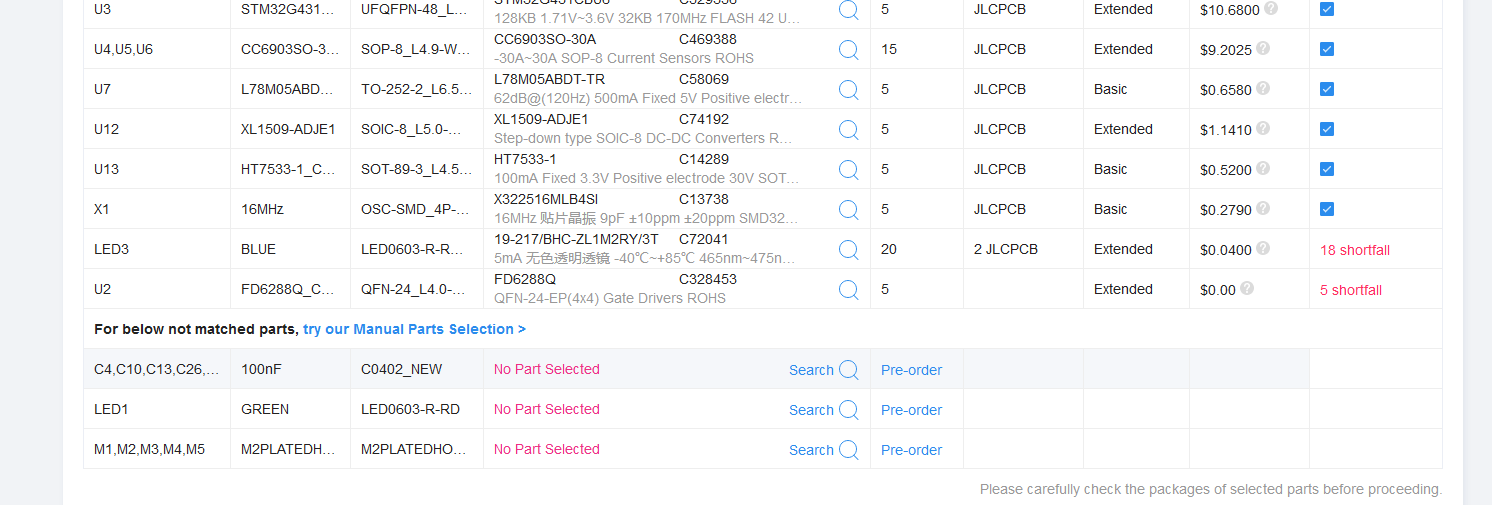
Sometimes JLC changes around PN or stock shifts. For the caps and LEDs, just hit the “search”, and enter in the specs (100nF, 0402, presumably like 50V or something for rating) and pick whatever they have.
The M1/M2… are just mounting holes, these can be left out of the bom, there is no part to place.
1 Like
There are too many blue leds, there is only one per board in the schematic :(. IDk if that’s a problem.
I dig the connectors can be left out.
The driver boards won’t be easy to just replace tho, do they go get them?
Probably minimum order quantity on the blue LEDs. Even if your order doesn’t use that many, you still pay the price, but it’s so low it doesn’t really matter.
FD6288Q out of stock is a showstopper though. Usually they have thousands, so somebody must have made a very large order or something. Hopefully more on the way soon. There are plenty available on ebay, but they’re more expensive and it would be a pain to solder them yourself.
1 Like
Yeah it’d be impractical to do them myself, I’ll have to wait till they are back in stock, if I order now do they hold it till they are in stock or do I have to just check back regularly?
I set a reminder to check in a week to see if they have things working, thanks for the advice y’all, I plan to order just minimal number of qvadrans boards exactly as they are and see how it goes. Then I think I will replace some of the connectors and might add small snubbers or whatever seems warranted, try to implement that thing we talked about re flooding the copper leading too and from the mosfets, things like that.
I think we are really on to something. The odrive micro is the closest thing right now and it’s way out there re price and stuff. There are really a lot of applications for a good board and even the integrated chips and stuff don’t work for a lot of things, it’s just gotta be reprogrammable.
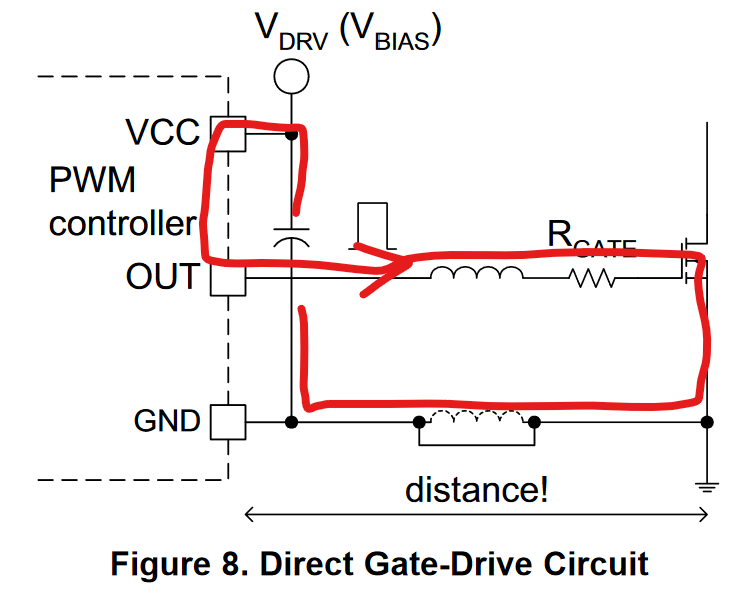
Looking at the QVADRANS design, I think there will be ringing problems on the MOSFET gates. The reason for this is because when designing the gate drive traces you need to minimise the parasitic inductance between the gate driver and the gate, to reduce the ringing. I have attached a screenshot showing the high current loops, which need to have minimal inductance. Image from TI’s Fundamentals of MOSFET and IGBT Gate Driver Circuits.
The current flow during turn on:
The current flow during turn off:
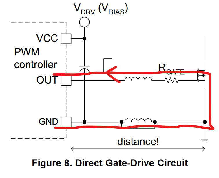
Now the inductance can be reduced in three ways: by making the trace thicker, or by making the trace shorter, or by having the forward and return current go next to each other as close as possible so the inductance cancels out.
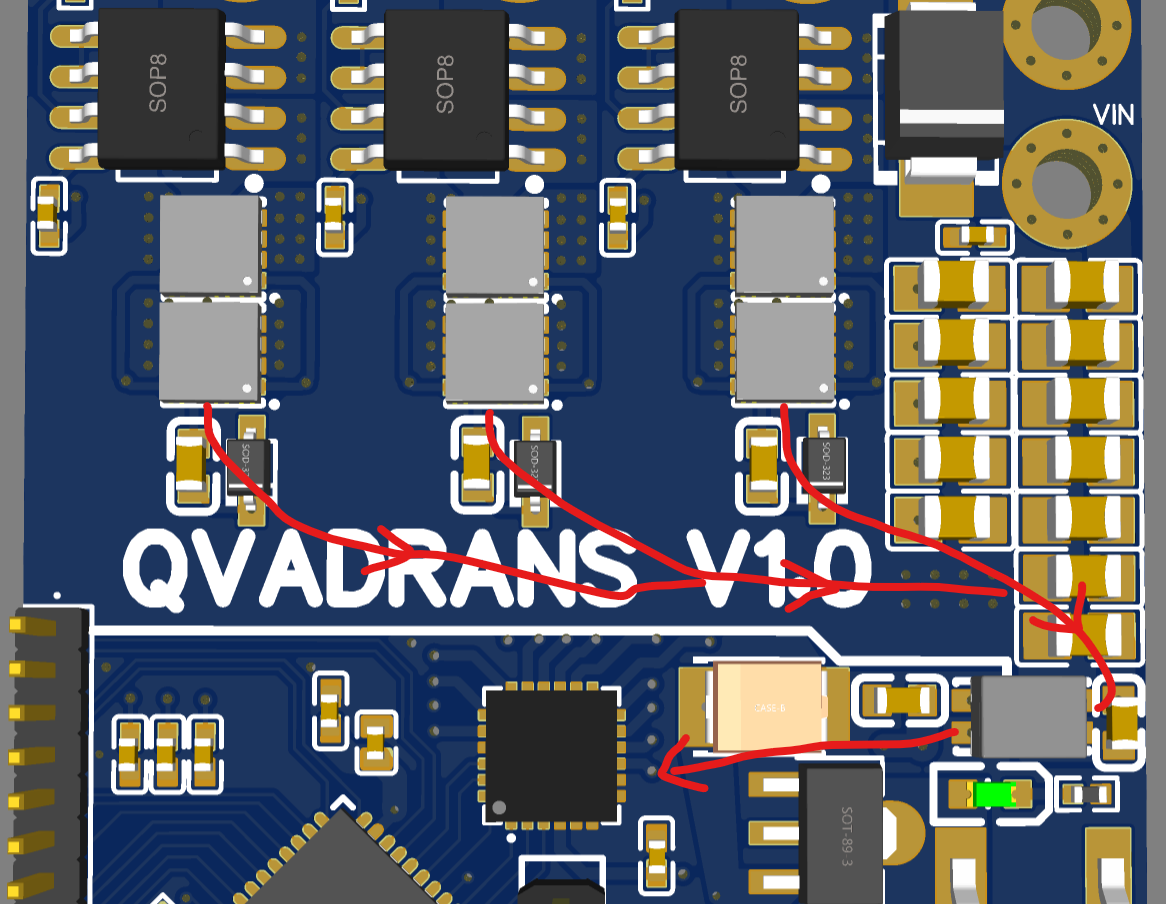
Unfortunately in the QVADRANS, the path of return current for the low side MOSFETs is very bad, it has to make a large loop around the board and go through an inductor (due to incorrectly split GND), before making its way back to the gate driver.
In my motor driver design, I have routed the gate traces very carefully, and I have got turn on and turn off times (VDS) of 20ns without any ringing on VGS or VDS. However my scope is only 100MHz bandwidth (SDS1104X-E), so I’m not sure whether the lack of ringing is due to good board design or due to the scope not having enough bandwidth to show it.
It should be a simple fix, just remove the split GND and the filter. In my experience using a single GND, I do not notice additional noise in the ADC readings when the MOSFETs are switching, so I don’t expect this change to affect the analog performance.
1 Like
How do I remove the “split ground”? Sorry, I’m really not the person to be doing this stuff, I’m just doing it because I need it done…
I can thicken the traces and move the driver a little closer but not much.
I assume the filter is there precisely because of the problems the lepton 2.0 had, but that was probably ringing. Definitely reducing the noise at the source would be better than trying to filter it.
The goal of my designs is educational, so people are free to improve on it.
Thank you for looking into my designs! Let’s hope others follow your suggestions.
Cheers,
Valentine
1 Like
Redo the GND pour, and replace all the DGND with GND, and remove the filter.
If you’re unsure how to do this, I would suggest taking a look at one of my designs. My version 4 motor driver is based on drv8316 and is fully validated with no issues, and my version 5 motor driver based on the drv8323 is almost ready, but is currently suffering from CSA offset issues, so I wouldn’t recommend ordering it yet.
That’s not true, but I don’t have time to respond now, I’m at work. Please check again.
Cheers,
Valentine
Hint: the board has 4 layers.