NEMA23 CNC FOC Stepper Driver Dev

PIN assignment:

The two current sense ANALOG input are assigned to ADC12_INP4 and ADC1_INP2, which should make it possible to use the dual ADC mode, for simultaneous samples.

That leaves ANALOG temperature (thermistor) port and ANALOG voltage_divider (BUS voltage) port on ADC3.

The HALL and ENCODER interface is on TIM3 CHA 1-3

All BLDC PWM signals are on TIM1 (Advanced Timer). Supports 4PWM stepper and 6PWM BLDC.

Just looking :wink:

The question ad hand is does it need paste to reflow or is flux sufficient ! Will it self_align ? → This

How precise is → this, laser for micro_vias (0,1mm Ø * 0,3mm Ø)

This guy says no paste Combining high-temp and low-temp solder on the same board | Details | Hackaday.io

1 Like

From the looks of this, the paste does help in the smelt process, but I suppose it’s not strictly needed.

And here the self_align part;

Are you planning to solder it yourself? Otherwise the fab will know what to do, but I believe paste is normally used.

How many layers is the board? These BGA chips with pitch 0,5 or smaller are quite hard to work with, they’ll make your boards a lot more expensive…

Luckily the boards are only 20mm x 42mm, but I agree in that prototypes will be more expensive, since the fab house can´t pool the design. In bulk production, prices will drop exponentially. Of course the same can be said about the MCU itself. Regarding the price, the real question is, if it can compete, as a use_case specific alternative to the Portenta H7 Light.

For prototypes, I believe I will have to reflow the boards myself. I do have a reflow oven, so if it works with just a bit of flux, I think it could be done. The datasheet does not specify anything about stencil opening recommendations for this package.

Its a 4 layer design. Even though the MCU footprint itself is tricky, the routing actually becomes cleaner, since I connect directly to VIA_IN_PAD.

Knowing the reflow_temperature profile for those chips will make it easier to do.

@runger Do you think an external memory through QSPI is necessary. If so, then I think it could work with 6 layers. Perhaps the pins are taken, haven’t checked. Maybe a small SMD SD card? Priority is TIM1 and TIM3 for ENCODER/HALLs. Apparently the TIM3 can work in a synchronized way with TIM1 doing the FET switching.

We could do a Crowd campaign, but that would require SimpleFOC support and proof of concept, so prototypes are kinda needed.

I’m really surprised you can fit it on 4 layers - with 13x13 balls I’d expect at least 6 layers and blind vias. And even that probably won’t even let you access all the pins… I think normally chips like this need HDI designs and maybe stacked vias, but TBH I can’t find much good material on how to lay these out. If you have any pointers they’d be very appreciated!

Yes, well, blind_vias is another process on top of the micro_via laser mowing. If the vias are laser_burned through the stackup, I think they are less troublesome to fab. Or do you think they shoot each layer w. thou laser, before they are stacked. From what I gather, the 0.1mm laser hole, does not need filling, since the plating is enough to close the gap.

Edit: I think I can fit a onboard SD card in there, but it does require some re_routing. Is it really needed for motor control purposes. The great thing about an external SD card, is that the USB could boot up a folder on the PC/MAC, for programming the MCU by dragging a file and resetting. Another way is to just flash the devise through USB?

Another argument is the possibility to have a INIT document in the SD card, which can be changed and saved by the user w. stuff like, basic settings or routines.

I suppose one can define the two cores as one waking stream and another subconscious

I think once you want things like that you have to talk to your fab.

I can tell you for example, that PCBWay, whom I like to work with, wouldn’t do laser vias in any kind of normal process. It was only available for the PCBA HDI design process, which is a lot more expensive.

And I think the laser vias are just for relatively short depths, I don’t think you can just laser a 0.1mm hole in a 1.6mm PCB, but I could be wrong. But even if you can, the aspect ratio will be so tall, it will be hard to plate such a via, and it will be very fragile…

In a “normal” PCB you won’t get laser vias, and if you want blind vias, each level-pair will be its own drilling and plating run, and so add significantly to the cost.
And you can only place vias between layers that satisfy certain properties. E.g. you can go from layer 1 to layer 2, or from layer 1 to layer 4, or from 3 to 4, but not from 1 to 3, or from 2 to 4.
So I think to route out all the pins would need like a 12-layer PCB with 5 blind via runs - at that point I think you can just make it a HDI design, and it will even cost less.
But of course if you only need a “sparse” routing, where most of the pins don’t get used, you might have enough space to get traces in to all the pins you do need on even just 4 layers, or even using through holes…

I never said it was a normal process.

But sure, if I can get hold of the MCU, else it’s just wishful dancing.

Here is a good read on HDI stacked uVia: Everything You Need to Know About Microvias in Printed Circuit Design

If using stacked uVia’s, a thin PCB thickness is preferred.

The only way to sketch it up in kiCad is to align several microvías (blind/buried vías) pointing to the right layers. The only way to achieve different size anular ring between outer and inner layers. It may not be possible in KiCad. That may require a expansion, or plug-in. Edit: Just found out, that choosing Blind/burried vias in KiCad, lets you place them stacked. So various size annular ring between layers in a uVia stack is possible in KiCaD.

Edit: @runger You are right about the HDI perspective. I guess it is a mindset of sorts, if blind vias from layer one L1 to layer two L2 is possible, then routing below that via is suddenly possible and it opens up some new pathways.

Maybe 0.8mm is to fragile?

Mkay, using HDI ive kinda found room for a 64Mb QSPI NOR FLASH DRIVE. This could be used to boot a folder for config files.

It is sharing a stacked uVIA [Rosenbridge] with the MCU so it can only be done if the QSPI interface can be internally powered by 1.2v, without messing other pin power domain up. The IC can only tolerate op to 2v.

Under any circumstance the pins are there, so maybe a different routing for a different package.

Actually maybe the core voltage should be 1.8 or similar, and the analog_reference, shall remain 3.3v. ?

The STM32H747 has a low-voltage IO setup, that I have a hard time figuring out. When low voltage is set, does all low_voltage pin then work on core_voltage eg. 1.2 ? And the rest, those pins without _h specefication, on 3.3v ?

With a 133Mhz bandwidth, it can make some really dense samples for graphing :smiling_face_with_three_hearts:

Let say we allocate 4Mb for plotting variables in a JSON format. With a 64byte transfer, it leaves up to 62.500 datapoints.

Changelog:

The low_voltage QSPI pin scenario is to dodgy IMO. So I have chosen a 128Mbit (16MB) IC with a 3.6v rating, instead of the 2v rated BGA.

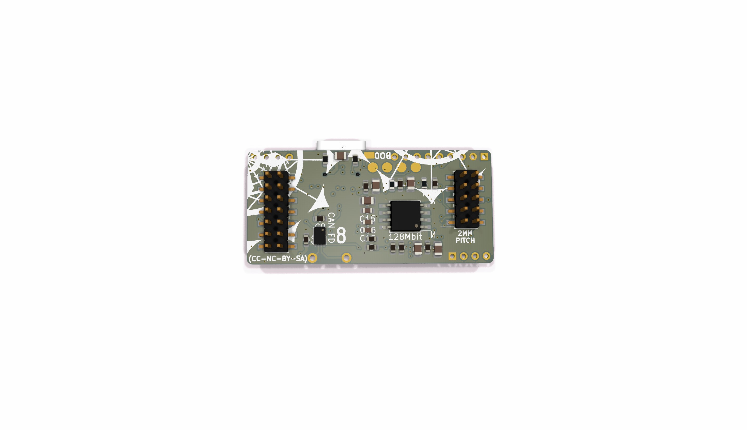
532MHz equivalent Dual/Quad SPI

If used for some science data acquisition experiment, maybe batterie powered, It will be a nice feature to have 16MB of external memory for logging. Maybe I should focus on the battery pin. Edit: The battery power pin is only for the backup domain, which has limited functionality. If powering the MCU for logging in the field, a USB battery should be used.

Comparing USB bandwidth/datarate with a QSPI memory for logging motor data is dificult. Especially if the USB interface is based on Serial (single char transfer) like the SimpleFocStudio. When doing single char transfers, the USB protocol overhead becomes a bottleneck.

In theory, the QSPI FLASH memory, can be divided into eg. 2MB sample segments, which enables testing a motor at eg. different torque settings or similar. Efter the test_run the acquired data can be compared.

Integrated driver class;

Have been playing around with the STspin32G4 MCU, which is a STM32G4 MCU with integrated gate_drivers. Since I sat out on this modular_design quest some moons ago, with this MCU in mind, it is only logical to integrate it into this new iteration of the modular format.

This MCU also integrate a buck converter, which handle all step-down needed for the gate_drivers. 48v NEMA17 driving should be possible with the right pre-requisite.

I think it is possible, also for stepper purposes. But in order to use it with steppers, a 4th gate driver must be used on TIM8 and it will require future SimpleFOC 8pin PWM support for steppers. Basically it will need a custom hardware specific setup for stepper purposes w. this unique MCU/BUCK/GATE_DRIVER. If used for 6pin PWM BLDC purposes, then the 4th gate driver could be used for eg. Brake_resistor.

Since the physical format is 42mm x 20mm this integrated driver class, should be a good fit for NEMA17 steppers.

Still a work in progress.

Preliminary pinmap, this may change.

At the two-yard peg she faced round, and said, ‘A pawn goes two squares in its first move, you know. So you’ll go very quickly through the Third Square—by railway, I should think—and you’ll find yourself in the Fourth Square in no time. Well, that square belongs to Tweedledum and Tweedledee—the Fifth is mostly water—the Sixth belongs to Humpty Dumpty—But you make no remark?

‘I—I didn’t know I had to make one—just then,’ Alice faltered out.

‘You should have said, “It’s extremely kind of you to tell me all this”—however, we’ll suppose it said—the Seventh Square is all forest—however, one of the Knights will show you the way—and in the Eighth Square we shall be Queens together, and it’s all feasting and fun!’ Alice got up and curtseyed, and sat down again.

At the next peg the Queen turned again, and this time she said, ‘Speak in French when you can’t think of the English for a thing—turn out your toes as you walk—and remember who you are!’ She did not wait for Alice to curtsey this time, but walked on quickly to the next peg, where she turned for a moment to say ‘good-bye,’ and then hurried on to the last.

How it happened, Alice never knew, but exactly as she came to the last peg, she was gone. Whether she vanished into the air, or whether she ran quickly into the wood (‘and she can run very fast!’ thought Alice), there was no way of guessing, but she was gone, and Alice began to remember that she was a Pawn, and that it would soon be time for her to move.

(Il y a du vrai dans votre fiction et du faux dans votre vérité)