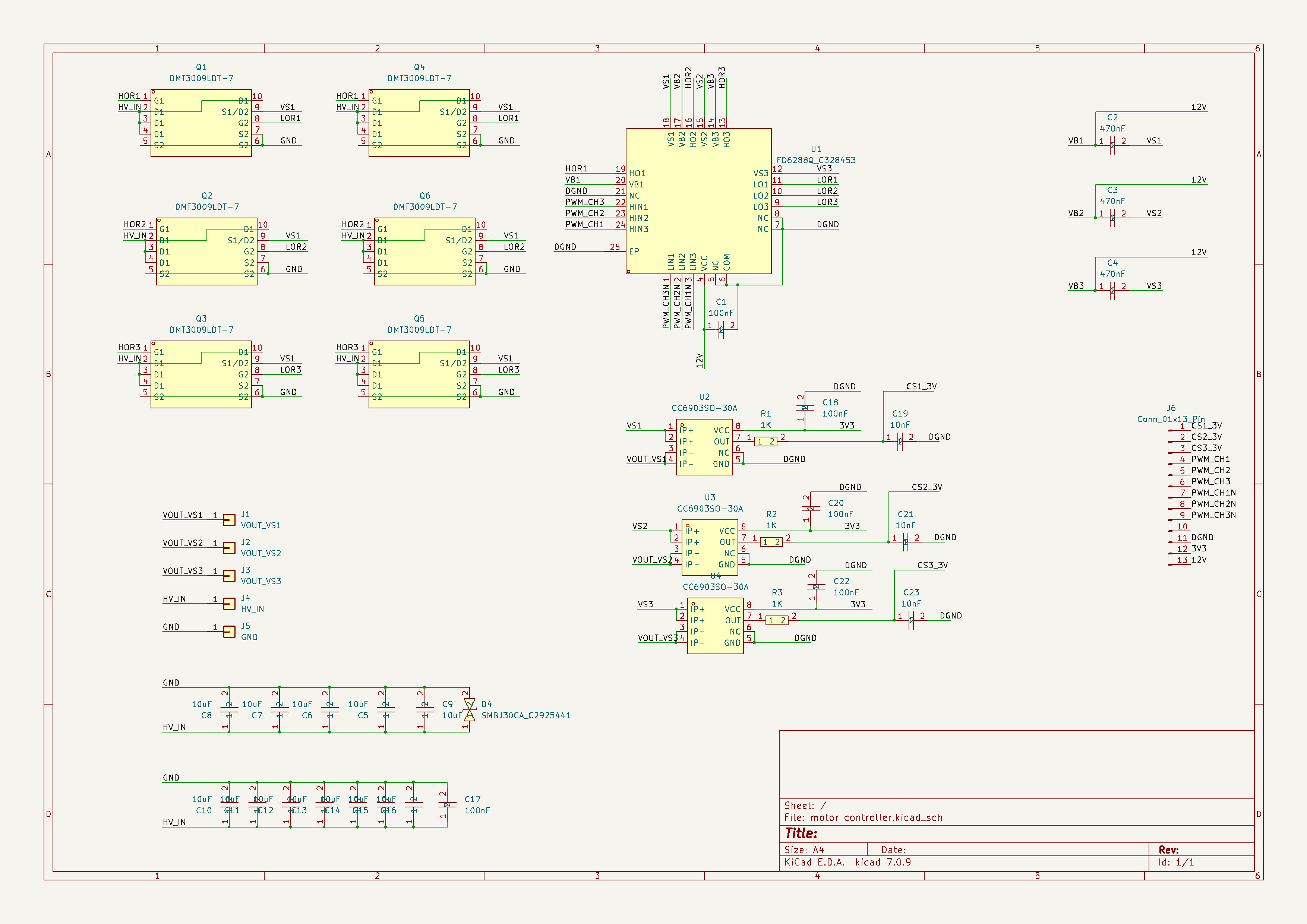
I’m working on a mini QVADRAN board with no MCU onboard, intended to be a stripped down version that is completely controlled an external MCU. This board is intended to be a learning exercise, or educational version of the board by @Valentine, with no frills or fancy features, besides those needed for basic operation. It’s intended to drive BLDC high performance motors, like the original board.
Any tips on this design so far? I’m planning on starting to route a two layer board soon, but I would appreciate any advice and suggestions with what I have so far.
I don’t really see where your DGND and GND are connected - maybe I missed it? The Fortior driver is not an isolated part AFAIK, so the input and output side do have to reference the same GND potential…
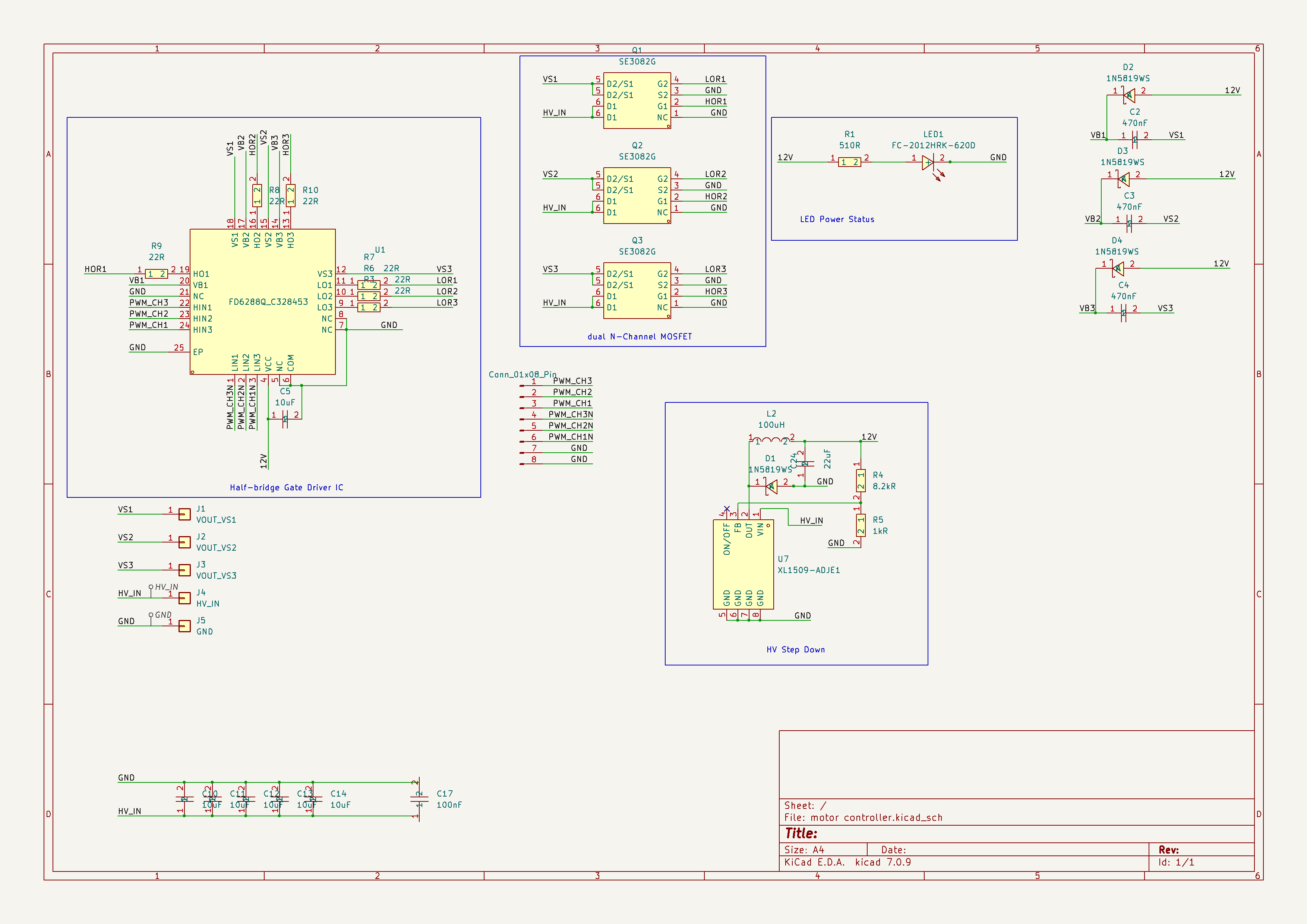
Personally I would add a power LED to let you know the board is alive.
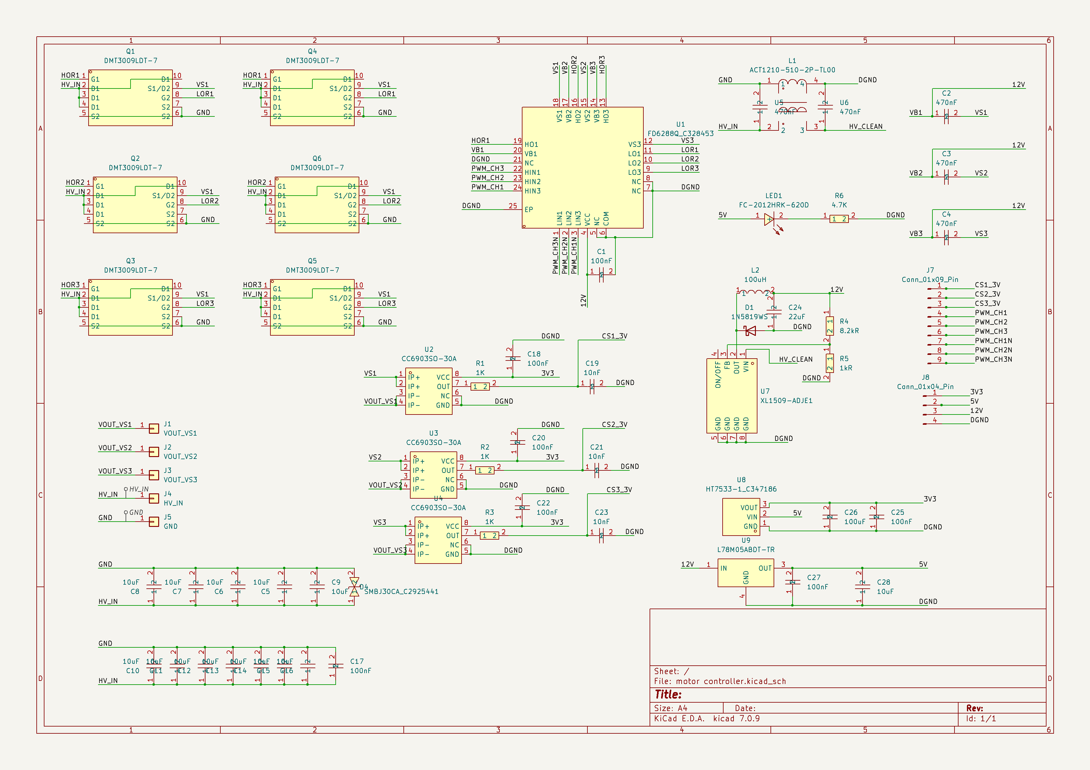
I’d also consider the power requirements, you have a “HV” rail, a 12V rail and a 3.3V rail. While HV will come from your motor’s power source, and 3.3V can be expected to be supplied by most MCUs these days, the 12V power will have to come from an additional source.
Here I find Valentine’s design on the Quadrans where the drive voltage (e.g. the 12V) and the 3.3V are generated from the HV input much more convenient to use… with that kind of setup you don’t even need additional power for the MCU board, you can just power it from the 3.3V rail of the motor driver board.
But I know it depends on the use-case, and yours may be different.
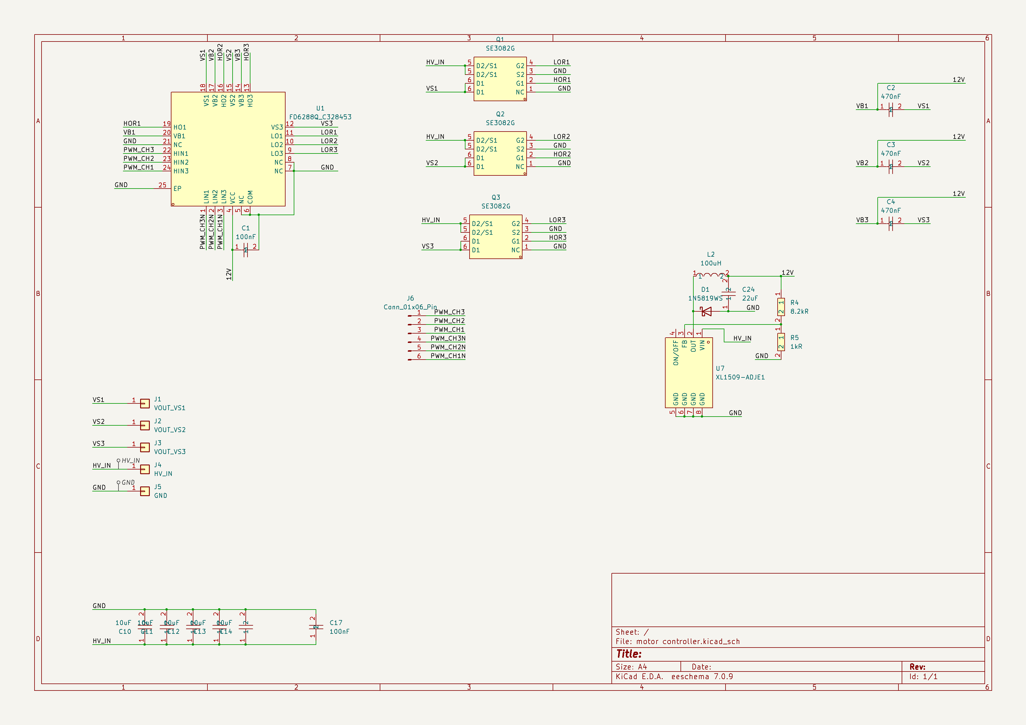
On second note, I’m probably should have picked an easier design for my first pcb to route. I’m going to switch to the Lepton v2 driver with integrated h-bridge driver mosfets instead. It looks rather difficult to route something as complex as this on a 2 layer stackup.
If you are planning to get these produced by JLCPCB, 4 layers is only marginally more expensive (maybe $1-2 more total for 5-10 boards), I would really recommend looking into how to do 4 layer and use that. Personally, I avoided it for so long because I thought it was complicated, but it’s really straightforward, it makes routing astonishingly easy, and solves so many noise problems from poor grounding. I wish I had started doing it earlier.
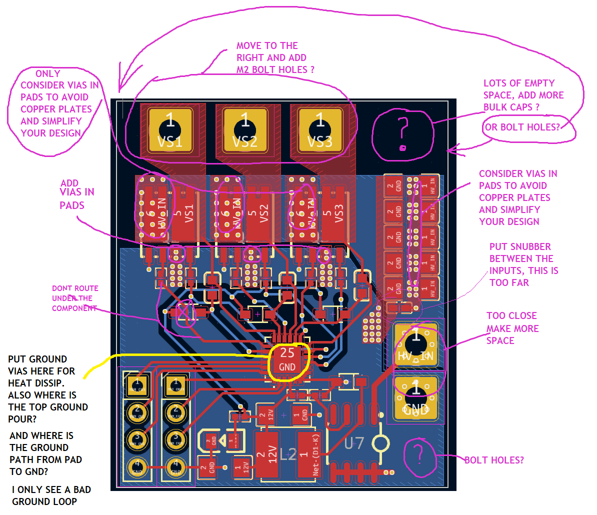
Something doesn’t seem right about the MOSFETs. You have have a different pin-numbering to the datasheet that I have, but assuming the pins are correctly labeled, then The HV_IN should be going to D1 (high side drain) and the phase signals VS1, VS2, VS2 should connect to the D2/S1 pins (the common terminal for high side source and low side drain).
Your 6-pin connector includes all the signals, but it does not include GND. But it will be necessary to connect the GNDs of the MCU and the driver boards. I would advise to add at least one GND pin to the input header.
As a side note, having some extra GND pins really can’t hurt. One GND for 6 signals isn’t being generous with GND
I like to include some LEDs to let me know the board is alive, but that’s just a personal preference, really…
Pin 4 of the XL1509 can be left floating according to the datasheet, but personally I would tie it to GND to make the intent clear, or mark it with the not connected ‘X’ in KiCad. The ERC checker tool will complain about it otherwise.
I agree very much with @VIPQualityPost about the 4 layers - 2 layers is really only suitable for very simple designs/boards. Forcing a design into 2 layers is often possible, but its doubtful the result will have good grounding, and may even develop signal integrity problems because of it.
It looks like you’re missing the diodes between 12V and VBx, and the 1-10uF capacitor between VCC and COM on the driver. See page 4 of the datasheet. You could add the recommended mosfet gate resistors too. It works without them, but may reduce the noise issues Anthony had and doesn’t add much cost or size.
@dekutree64
Choosing gate resistors turned out to be a bit harder than expected. I referenced this answer.
Rise time is 15nS with drive voltage being 12V and total gate charge being 51nC.
I_g = gate charge/rise time = 51nC/15nS = 3.5A
V/I = 12V/2.4A = 3.53 ohms.
Unfortunately, no reasonably sized resistors exist on LCSC, so I’ll have to find an upper resistance value.
Assuming a 32khz max PWM switching frequency, and 1% of one period of the pwm frequency being acceptable for rise times,
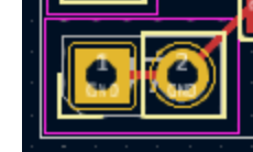
There are several places the routing is unnecessarily close. Try to increase the spacing:
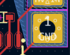
You have a lot of via in pad:
To do this correctly, the PCB shop has to fill these vias with resin, plate over them and then polish them flat. That’s expensive, it will add a lot to the cost of the PCB.
Otherwise, they can leave the vias open, but you run the risk that the soldering will not work reliably because the solder can run off through the vias. Or you can tent over them, but there is risk the soldering won’t work well due to trapped air.
I think the design does not need via in pad, and you could move them all out if you wanted.
Why not extend it across the whole of the board under the MCU and all those signal lines? As it is at the moment, none of your signals has a ground reference under it…
they should be in-between the other communications pins, so that the resulting cable has GND wires next to the signal wires. In an ideal world each signal wire would be twisted around a GND wire, like in an ethernet cable. But when using ribbon cables or individual wires, just mingle some GND pins in-between the signal pins so the GNDs aren’t too far separated from the signals.
These capacitors are connected only with a very thin trace and a single via. But these are part of the critical power path, being charged and discharged all the time as the FETs are switched on and off. They need big fat traces and many vias to GND/HV_IN.
Same for the traces on the buck converter. It’s true these aren’t carrying the same currents, but they’re still power connections - I would try to make them wider.
But it looks like its coming along very nicely!
Are you assembling the boards yourself or ordering them assembled?
Not sure but it looks like on your headers the separation between the two headers isn’t exactly 2.54mm in the horizontal. If you space them at 2.54mm like the vertical spacing, then it’s more convenient for users, they can use a 2x4 ribbon cable for example.
My comments. One other comment, these half-bridge integrated MOSFETS are hard to find, watch out, you might have a problem sourcing them. And please add bolt holes, the mechanical fastenings for motor boards are very important.
I’m a bit confused on why to put VIA in pads for the GND connections on the MOSFETs though. I thought having VIAs in pads would increase the chance of tombstoning, so whenever it is possible to avoid them, I didn’t have any via in pads, such as on the bulk capacitors. I had to add them on the HV_IN pads of the MOSFET since I can’t think of any other way to transfer the power to the MOSFTs though, or for heat sinking the GND of the MOSFET drivers.
I also added a ground plane to the top layer. I’m still relatively new to high power PCB design, but when is it normally useful to add power planes for either ground or VCC?
Besides that, I think I hit most of your points in your post. I moved the snubber cap, rerouted that trace going through a footprint, etc. Anything else I can alter before sending it off to a PCB shop?
@runger Thanks for the advice about spacing. However, I am unsure on how to route the three PWM inputs to the far pins with the edge of the board being so close to the edge. If you have any tips for doing so, it would be appreciated.
This is usually only true for smaller parts… the MOSFETs should have enough surface area to prevent them from pulling away, although they will still have the solder-wicking problems that @runger mentioned earlier.
I would say you should always try to use a ground plane on all layers, you likely don’t need a full power plane in nearly any case. If you need more current on a large power rail, just use a fat trace, even if it’s on an internal layer, IMO. There are calculators for this about trace width vs current.