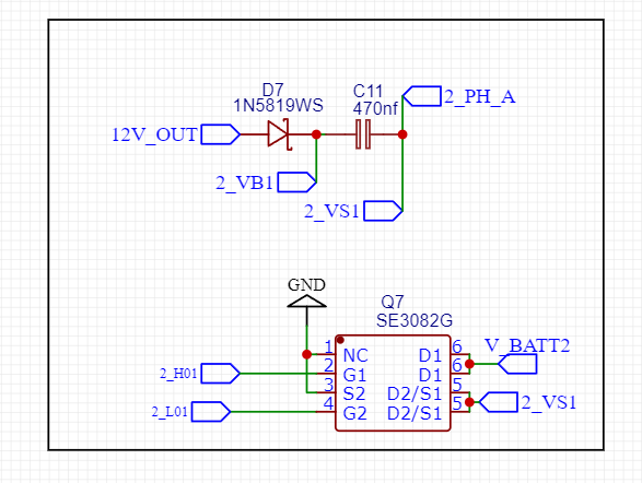
So the input to the D1 of the MOSFETs is now the V_BATT2 line, correct?
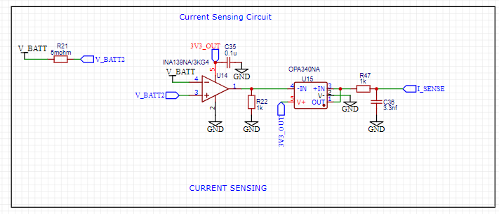
For the INA139 it looks in your most recent picture like the VDD input isn’t connected to 3.3V?
So the input to the D1 of the MOSFETs is now the V_BATT2 line, correct?
For the INA139 it looks in your most recent picture like the VDD input isn’t connected to 3.3V?
Regarding the current measurement circuit - the reason to use the OPA340 is as a buffer for the output voltage of the INA139 - but are you sure you need it? I’m not saying you don’t, and in principle it is probably the more “correct” way to do it, but I would expect the load resistance of the MCU’s ADC to be quite high, and therefore not affect the gain much. Also, you could probably calibrate for the effect it does have. So perhaps it’s an option to simply set the gain of the INA in such a way that you don’t need the buffer Op-Amp at all?
If you do keep it, I would have expected it to be wired as a voltage follower, with the input to the non-inverting terminal and negative feedback. But you have it wired as a “inverting follower”, with inverting input and positive feedback? Is that a valid configuration?