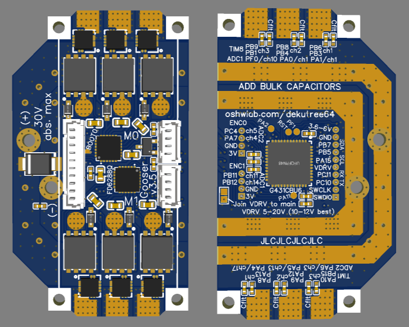
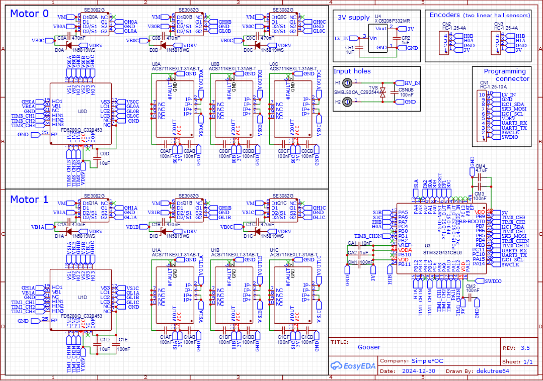
Ok, I’ve managed to gather a little more information. The drivers will run on 5V, and ESP32 pins are 5V tolerant, so I can safely probe everything when running on a 5V supply. The mosfet gates are receiving correct PWM signals. High side waveform matches the input pin, low side is inverted.
Probing the mosfet output seems to confirm what the multimeter shows. When high side gate is fully on, output is fully on, otherwise the output is almost fully off but with sporadic blips.
I also tried measuring the gate pins with the multimeter and they seem ok, except the high side gate is somewhat lower than it should be. With 5.09V power supply, 100% duty reads 4.1V, 2/3 duty reads 3.3V, 1/3 duty reads 1.5V. Trying with the 7.7V battery, 100% duty reads 6.7V, 2/3 duty reads 4.7V, 1/3 duty reads 2.3V. Corresponding low side gates are just as they should be, 100% duty 0V, 2/3 duty 2.5V, 1/3 duty 5.1V.
No clue what the problem could be. The mosfets are wired up just like Lepton, and receiving seemingly valid inputs, yet they don’t work.
I think it’s one or the other depending on mode. Inverting mode is INHx pulldown, INLx pullup (both mosfets off if input pins are floating). Which means that I actually could use hi-z/freewheeling if I disable the timer and configure its pins as inputs
But since the pins are externally connected, you get a voltage divider via the external connection?
Ok but this would indicate that the drivers are in fact working? What’s the threshold voltage of your MOSFETs and what happens if you go to 12V gate drive voltage?
Oh! You’re right. I doubt it matters since the signal from the MCU should overwhelm the ~200kOhm pull-up/down, but that does mean they’re in an undefined state at startup until the MCU pins are configured as output, and freewheeling mode is not possible after all. But the cross-conduction protection should prevent any real trouble.
Correct, the drivers seem to be working, but the mosfets are not. The datasheet says RDSon=7.5mOhm at Vgs=4.5V, 5mOhm at Vgs=10V. There’s a graph that I don’t quite understand, but seems to indicate threshold voltage is around 3.5-4V. So the 5V output probing results are somewhat suspect, especially with the high side gate seemingly only receiving 4.1V, but the 7.7V battery should be plenty to get it going. I’ve done a lot of motor testing on Lepton with it.
I tried with a 3S lipo (presently charged to 11.7V) and got similar results. 100% duty reads 11V on the mosfet outputs, lower duty is around 100mV or less. Gate voltages show a similar pattern as before, with high side being a bit lower than expected. High side 100% duty->10.6V, 2/3->7.4V, 1/3->3.7V. Low side 100%->0V, 2/3->3.8V, 1/3->7.7V.
Thanks for all your help so far! Hopefully we’ll get to the bottom of it eventually.
EDIT: Tried setting PWM frequency 1KHz and made no difference. I thought maybe since the mosfets do seem capable of switching on and off, doing so at a slower speed might help.
EDIT2: Next test: Ultra-low frequency. No more timers, just set the pins to output mode and use digitalWrite to switch them on and off, and then probe mosfet output with ESP32. Even at one on-off cycle per second, the output is asymmetrical (more off-time than on-time), and it gets progressively worse until 8Hz there’s almost no on-time left, and 16Hz+ there is none visible at my fairly low resolution of 244us per pixel. Mofset gates are still good, and the output waveform matches the input frequency, it just seems to be very slow at switching on.
Correct me if I’m wrong, but the high side FETs are usually switched via a bootstrap circuit. That often requires external component(s). Maybe they’re too tame to boost the FETs?
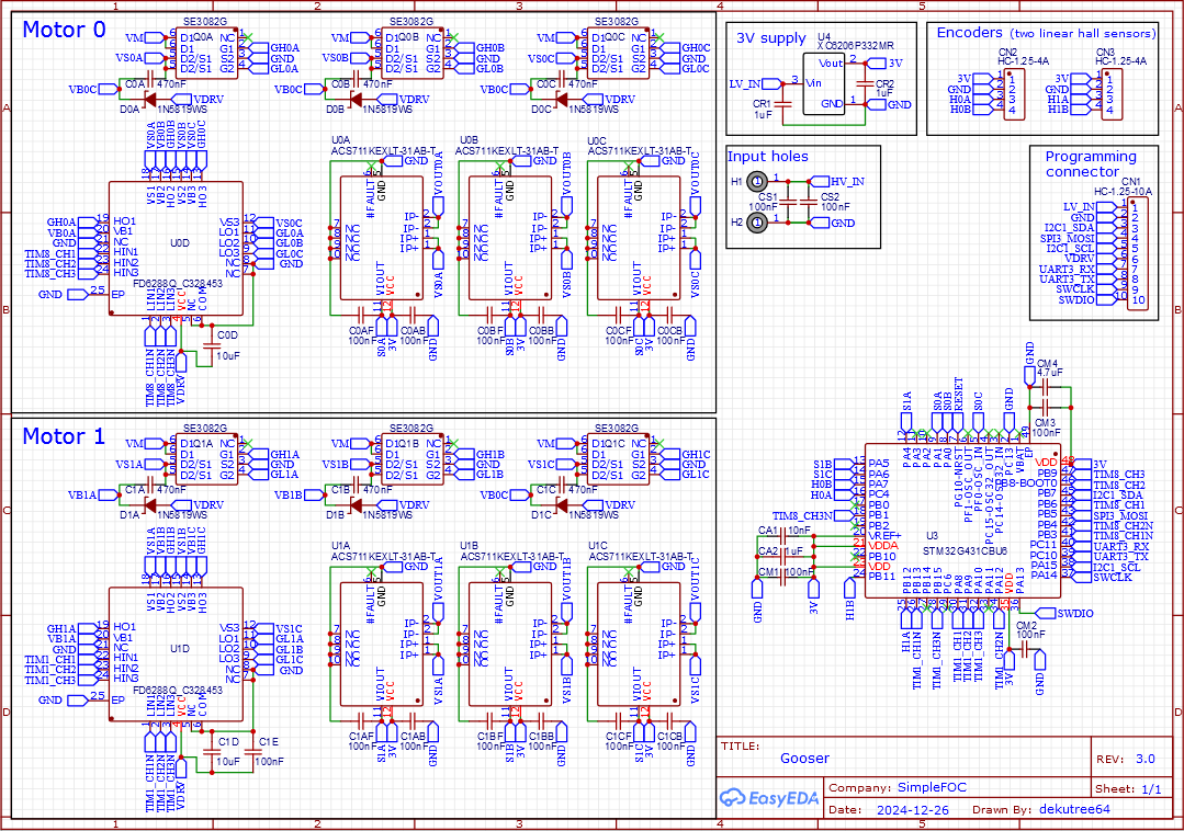
The DRV8300D has the bootstrap diodes integrated, only the capacitor is needed externally.
But of course the bootstrap can be a source of problems, esp. at 100% duty cycle.
You can check it by checking the capacitor against GND, it should charge up to Vmot +Vbst every cycle. Using an oscilloscope I mean.
Yeah, 5V sounds like too little but 7.7 is probably ok on 4V threshold.
We’d have to do some math to see how quickly the gate charges up in these conditions.
But if it worked on Lepton for you then probably there’s another issue to discover.
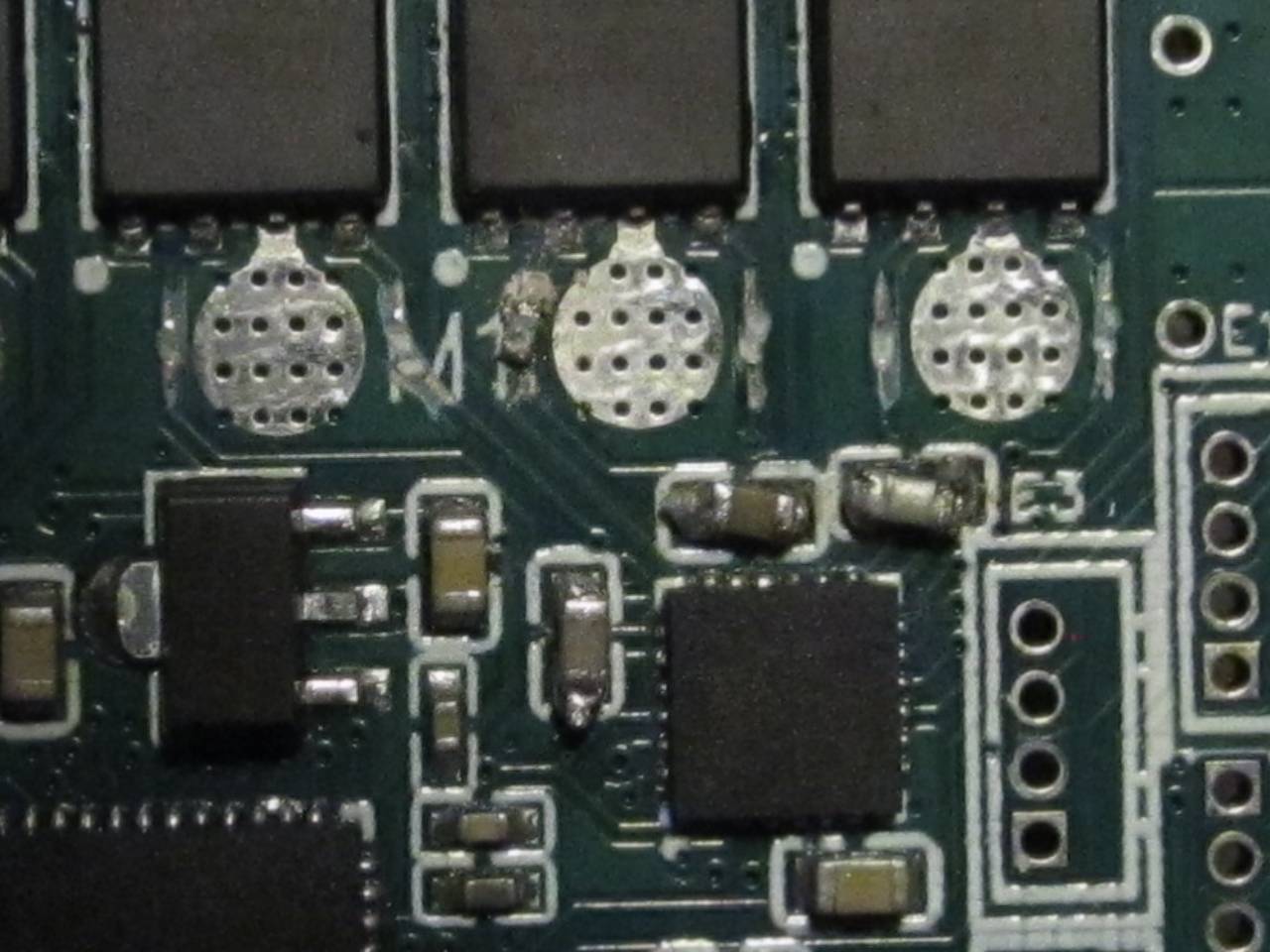
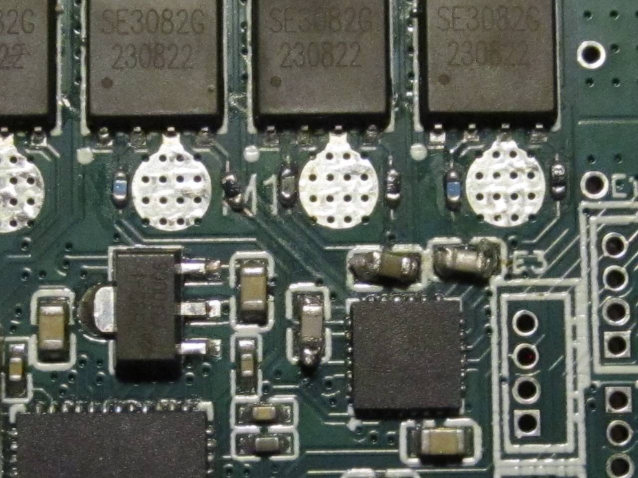
Ok, I have some actual oscilloscope measurements now. PWM frequency is 25KHz and measures correctly now. Apparently I was doing something wrong on my ESP32 when it seemed to be doubled.
Battery 7.7v
100% duty:
Low side gate 0v
High side gate 6v
Bootstrap capacitor 3.5v
Mosfet output 6.4v
2/3 duty:
Low side gate alternates 0v and 8v
High side gate alternates 0v and 7v
Bootstrap capacitor is mostly 7v, with 230ns blips up to 10v
Mosfet output is mostly 0v with 230ns blips up to 3.4v
1/3 duty:
Low side gate alternates 0v and 8v
High side gate alternates 0v and 7v
Bootstrap capacitor is mostly 7v, with 230ns blips up to 13v
Mosfet output is mostly 0v with 230ns blips up to 6.2v
The blips seem to occur during the deadtime window, starting as the high side gate is switched off, and ending just before the low side gate is switched on.
For comparison, I took the same measurements on Lepton:
Low gate alternates 0v and 8v
High gate alternates 0v and 15.5v
Bootstrap capacitor alternates 7.4v and 15.2v
Mosfet output alternates 0 and 7.7V, with small spikes at the transitions to about 8v and -0.3v.
So apparently the bootstrap is not working, but I still don’t know why.
Yeah, this really sounds like an issue with the bootstrap capacity. With the exception of the 100% duty cycle test, which is an edge case, they should charge up to around 15V (2x your VM) each cycle. And they should charge both during the dead-time and the low side on-time, not just during the dead-time.
Are the caps used actually 470nF like in the schematics?
You could try replacing all the 470nF caps with 100nF ones and see if it helps? I wonder if it’s an issue that the total capacitance is 4x that of a single driver? If the drivers are all switching in sync?
But probably you’re testing only with one driver active at the moment?
Results are the same whether one driver is running or all four. I may sacrifice a board to try adding gate resistors (though I’m not terribly confident I can solder to a 0.15mm trace…), and in that case I could try changing to 100nF capacitors while I’m at it.
I’ve pretty much confirmed that the internal diodes are not the problem. I used a jumper wire to connect a diode to battery+, and manually touched it to the bootstrap capacitor terminal. The mosfet output blip remains basically unchanged, aside from a slight drop in amplitude while the diode is in contact.
Transplanted DRV8300 onto a Lepton to see if it would run. Results inconclusive but not encouraging.
I took a Lepton with burnt mosfet and removed that mosfet, the FD6288Q driver, and two of the bootstrap diodes (one left to see if it makes any difference). Removed one driver and mosfets from the Gooser and transplanted them onto the Lepton (after some surgery to the PCB to disconnect the mode and DT pins, which were unused/connected to ground on FD6288Q).
When I first powered on the Lepton, I heard a snap, and the newly transplanted mosfet now has a bubble on it, as they do when burnt. I then discovered I had uploaded a bad .bin, but I don’t think it would have activated any driver inputs so I don’t know what happened.
Probing with the oscilloscope, the driver inputs from the CPU are all good, but outputs to the gates are not. Only the phase with the probably-burnt mosfet is working. The other four gates never change. I can’t find any solder shorts with the multimeter, but wouldn’t be surprised if it’s a soldering problem, or heat damage from reflowing 3 times now (including the initial assembly by JLC). The probably-burnt mosfet acts just like all the ones on Gooser, so it may still be functional. Output mostly 0v, with blips during deadtime, and bootstrap capacitor sitting at battery voltage with matching blips above that.
The last thing I can think to try is adding gate resistors, but I don’t have any on hand so I’ll have to order them. The various gate peak current ratings in the datasheet have quite a wide range (400mA to 2100mA), but I think 500mA should be a safe target. My final battery voltage will be 13.2v (4s LiFePO4), so maybe 25 ohms? With the 7.4v battery I use for testing, that would be 300mA, or 170ns to charge the 51nC gate, which is cutting it a little close on the ~200ns dead time, but probably ok for testing.
The gate resistors arrived today, and still the behavior remains the same. However I have gained some confidence in my soldering abilities It turns out soldering 0402 resistors to 0.15mm traces is not so hard after all.
I used a 0.3mm wide chisel made from an x-acto knife blade to remove the soldermask, and to stab through the trace in two places and pick out the bit of copper. First I did a single high side gate by hand using a fine tip on the soldering iron. Apply two dots of paste with a toothpick, place the resistor with tweezers, hold it down with a toothpick, and touch the iron to each terminal to melt it. Successfully done, but no change in behavior, so I decided to try doing all 6 incase it was going into an overcurrent protection mode or something.
The reason for the different colors is that DRV8300 has higher current rating for low side so I bought 17 ohm and 25 ohm. And the middle high side that I did by hand is upside down, showing its un-colored side.
I’m all out of ideas at this point. It’s wired up exactly like the datasheet shows, and it still doesn’t work. I think I’ll have to redesign with a different driver and transplant the rest of the components.
Thank you, that is very generous. I’ll keep trying on my own until then. Knowing that it works on Qvadrans is a big help. The setup is almost identical aside from the use of 3PWM mode, and I have confirmed by two-channel oscilloscope that the mosfet gates are receiving inverted signals with proper timing. The only problem is the high side gate is not boosted to double voltage.
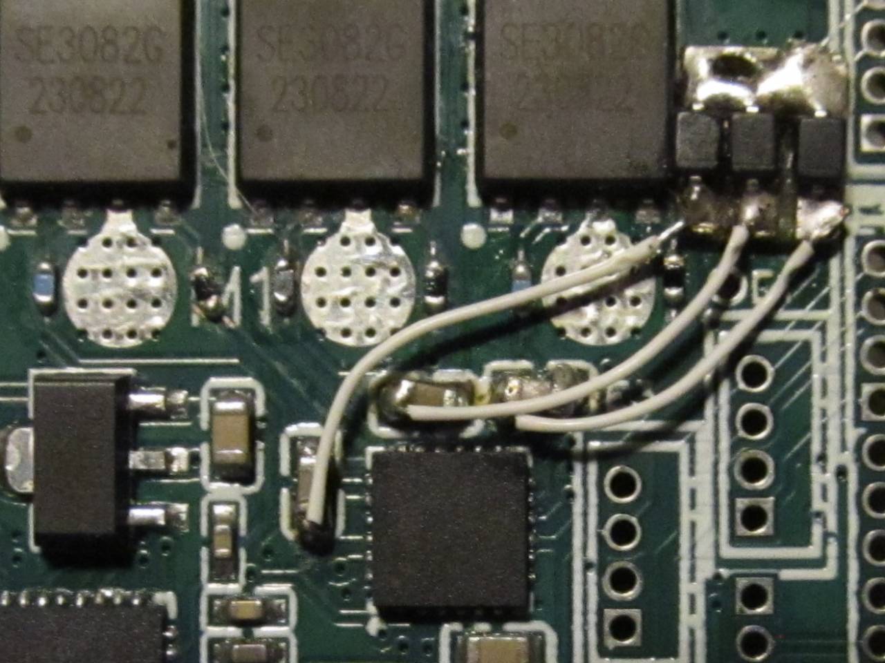
Today’s testing: Plucked the diodes from a Lepton with burnt mosfet, and put them on a little daughterboard which is connected to +V with a short wire though one of the bulk capacitor holes, and to the bootstrap capacitors using 34awg wire. No change in behavior.
My foggy understanding of the bootstrap/charge pump is, that it needs a separate oscillator apart from the gate-PWM.
Do you have to config/enable this internal oscillator somehow?
I’ve decided to throw in the towel on this one. Nomatter how much I go over the circuits, there’s no reason it shouldn’t work, and yet it doesn’t.
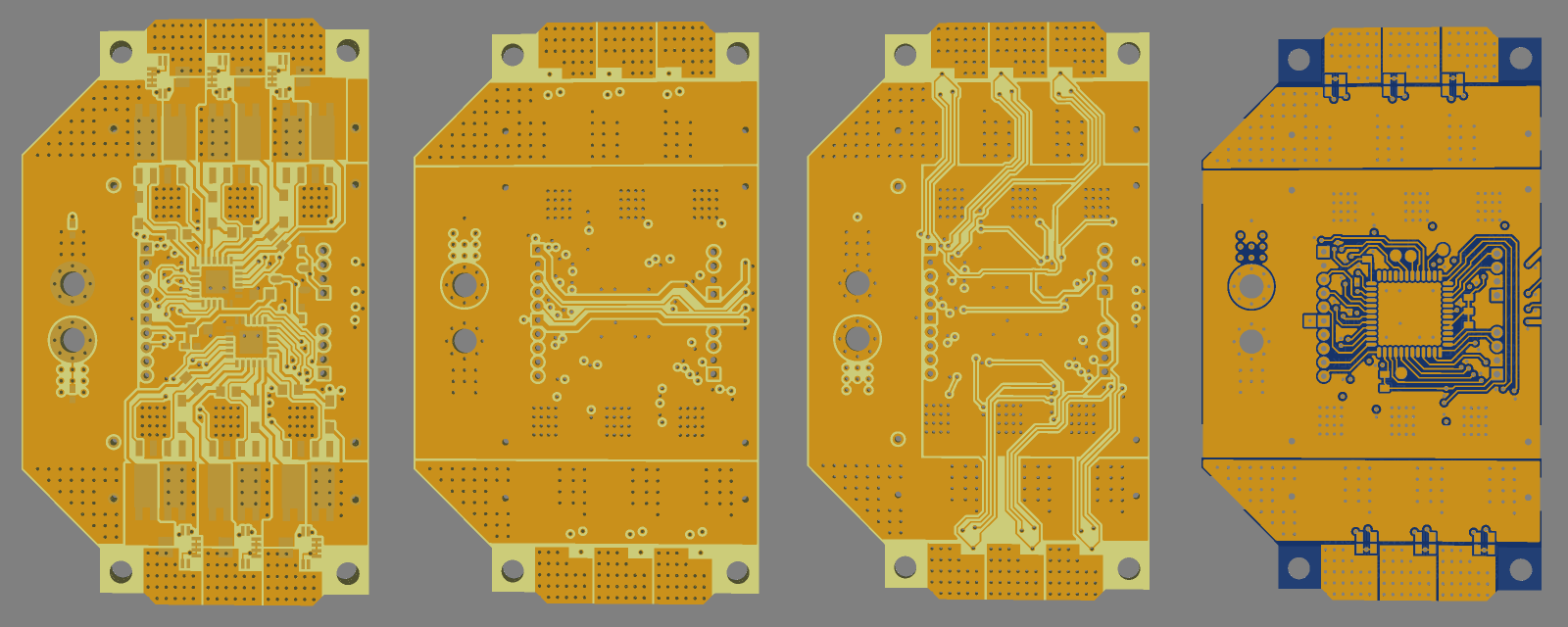
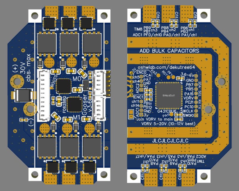
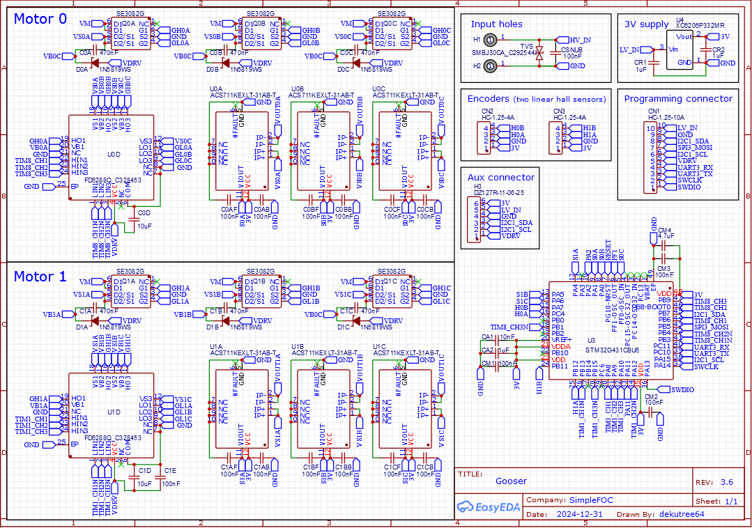
And aside from that, after setting up some motors on B-G431B-ESC1 and getting a feel for the G431’s processing power, I think it would be a bit slow for four motors anyway. So I started fresh with a dual-motor version using 6PWM on FD6288Q with external bootstrap diodes, pretty much identical to Lepton. This also gives enough pins for 3-channel current sense. There are some other changes too, like the ability to supply the driver voltage separately from motor voltage which enables using it with the 24V power supply on my lathe It’s running fine with B-G431B-ESC1 for now, but I expect the big hoverboard motor will kill it sooner or later (might kill Gooser too, but at least it’s cheaper and more repairable).
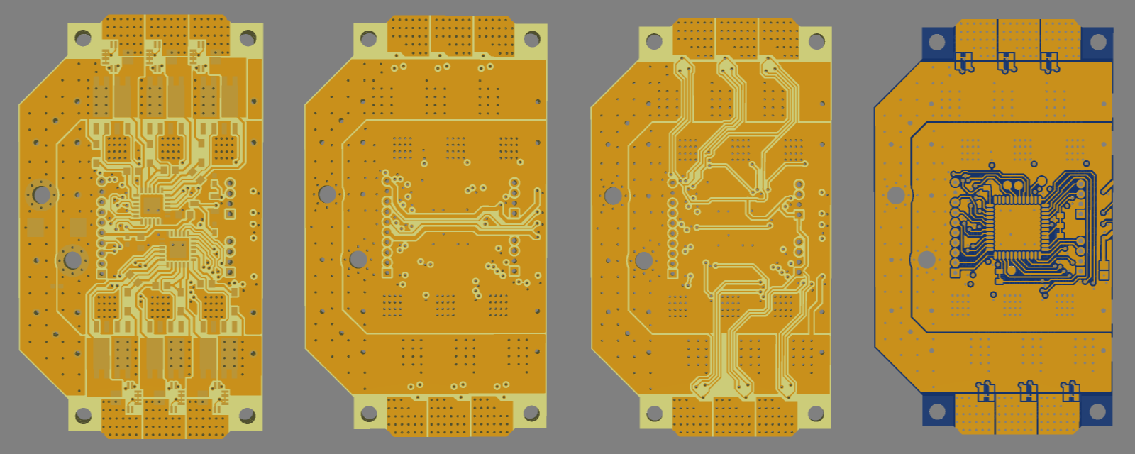
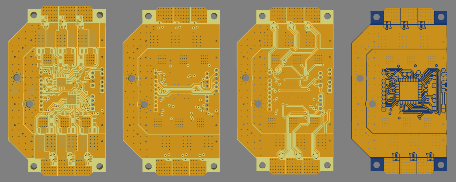
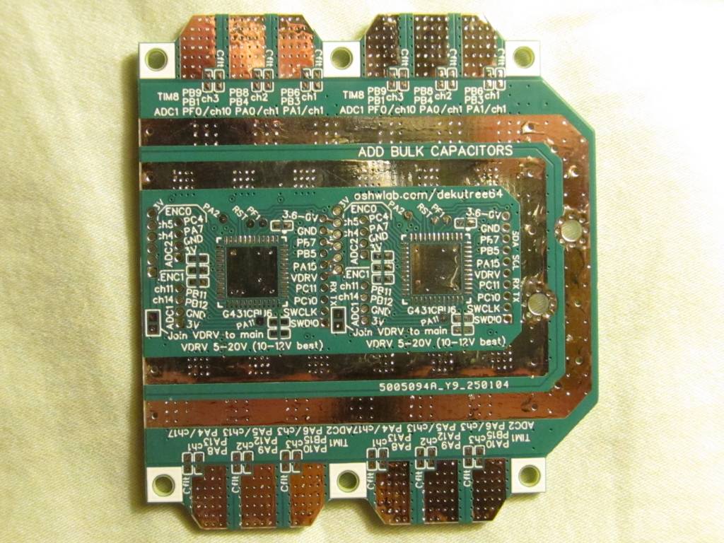
I originally designed it as a 20mm wide board with 2mm margins, with the intent to solder two side-by-side on copper bars to get a similar 4 motor layout as before. But then I came up with an even better way to connect them, by copy-pasting in EasyEDA and manufacturing as a single board. You can actually paste as many as you want, and edit the input terminal area as necessary for the higher current.
I had to move the CPU to the back side to keep it this compact, so it’s basically full double-sided assembly now. I’ll be assembling them myself anyway, transplanting components from the old boards.
I decided to see if I could squeeze in the TVS diode from Qvadrans, and in the process realized that there’s no real need for the input terminals to be positioned as they were. In addition to stuffing the TVS between them by widening the vertical spacing, I also shifted them horizontally to open up the power rails much better. I was even able to reduce the board width by 1mm while keeping the vertical rail cross section roughly equal to the horizontal rails (equivalent to 12mm width of 1oz copper), plus the positive rail is exposed on the back for the option to add U-shaped copper bars or more ceramic capacitors. Unlike GooserCS, the bars would cross over the input terminals, which may or may not be a bad thing.
I think I’m happy with it now, but I’ll sit on it for another day or two before ordering incase I come up with any more bright ideas.
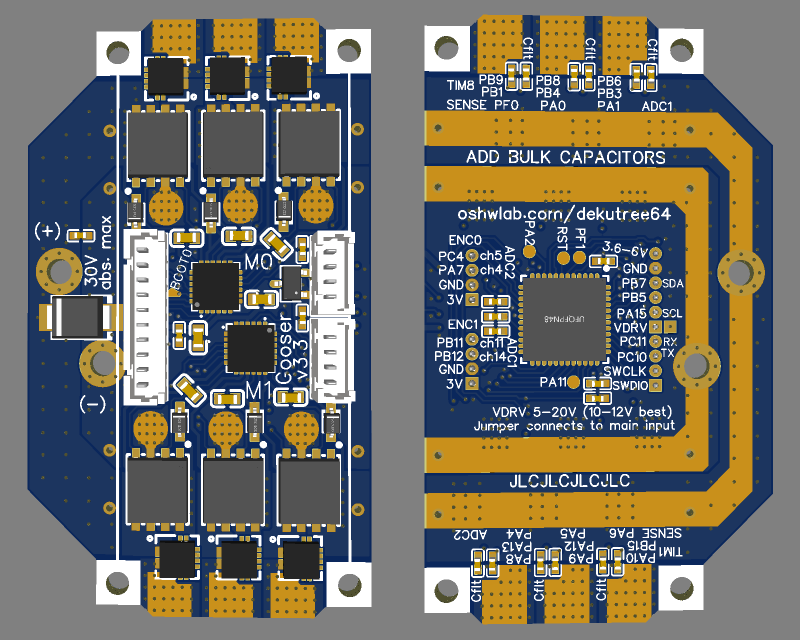
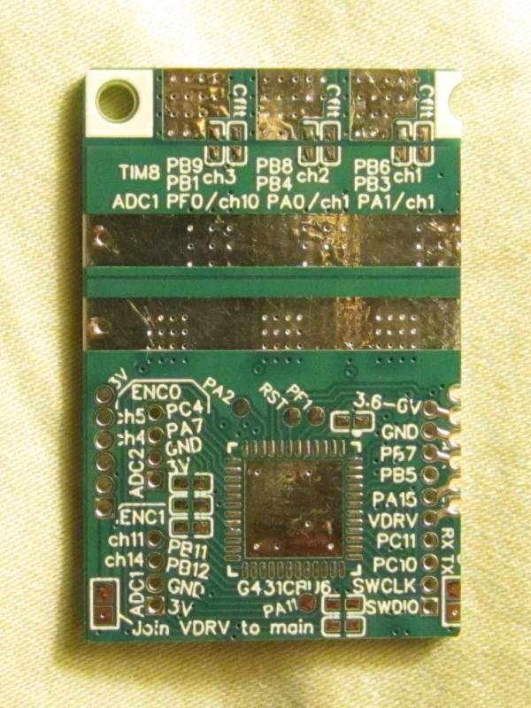
Managed to scoot the 3V regulator 0.2mm farther to the left. It was bothering me that it was so close to the encoder pads. It wouldn’t be a problem if using actual connectors, but bare wire ends are easier to route through all the actuators on my robot so I’ll be soldering them directly to the board. I wish it could go a little farther, but even this was a challenge. Had to scoot the driver chip 0.15mm to the left as well, and shift around a bunch of tracks and vias.
Edited exposed copper areas to give more options for exact placement of copper bars and ceramic capacitors, better placement of ground bars under mosfet vias, and added more holes to give more options for placement of through-hole capacitors and position pins for bars.
That necessitated moving the VDRV solder jumper away from the ground rail. It’s in the lower right margin now, so it will get chopped off if you want to use the board at its minimum 20mm width, but moving it does have advantage of giving the ground rail a touch more cross section.
Moving the exposed copper area also revealed that I had a mosfet gate via dangerously close to being exposed. Scooted some things around to move it and another one further inland.
As on GooserCS, I’ve extended the motor wire pads so the bottom board’s can protrude for easier access, and added some holes over on the edge for connecting necessary lines between stacked boards. But this time I realized I don’t need to get all the encoder pads accessible on the top board. I feel silly for not noticing before, but only the battery on my robot obstructs access to the bottom board, and it is removable. I can solder encoder wires to the bottom board no problem. They’ll also be much more spread out this way, so easier to work on.
Always good to have some spare time between the years.
I’m a bit concerned about your 4 motor design. The power-traces are same size as before, but are twice the length and carry twice the current.
Maybe better to add another battery connector on the left side and use a split battery-harness?
You could, but soldered-on copper bars are more elegant and carry the current right to the mosfets rather than just to the input terminals. And in my case these drivers are overkill for all but two of my motors, so I probably won’t need bars if I put put the largest and smallest together on one board and the middle sizes together on the other. Otherwise I’ll do the largest four on one board with bars and smallest four on the other without.
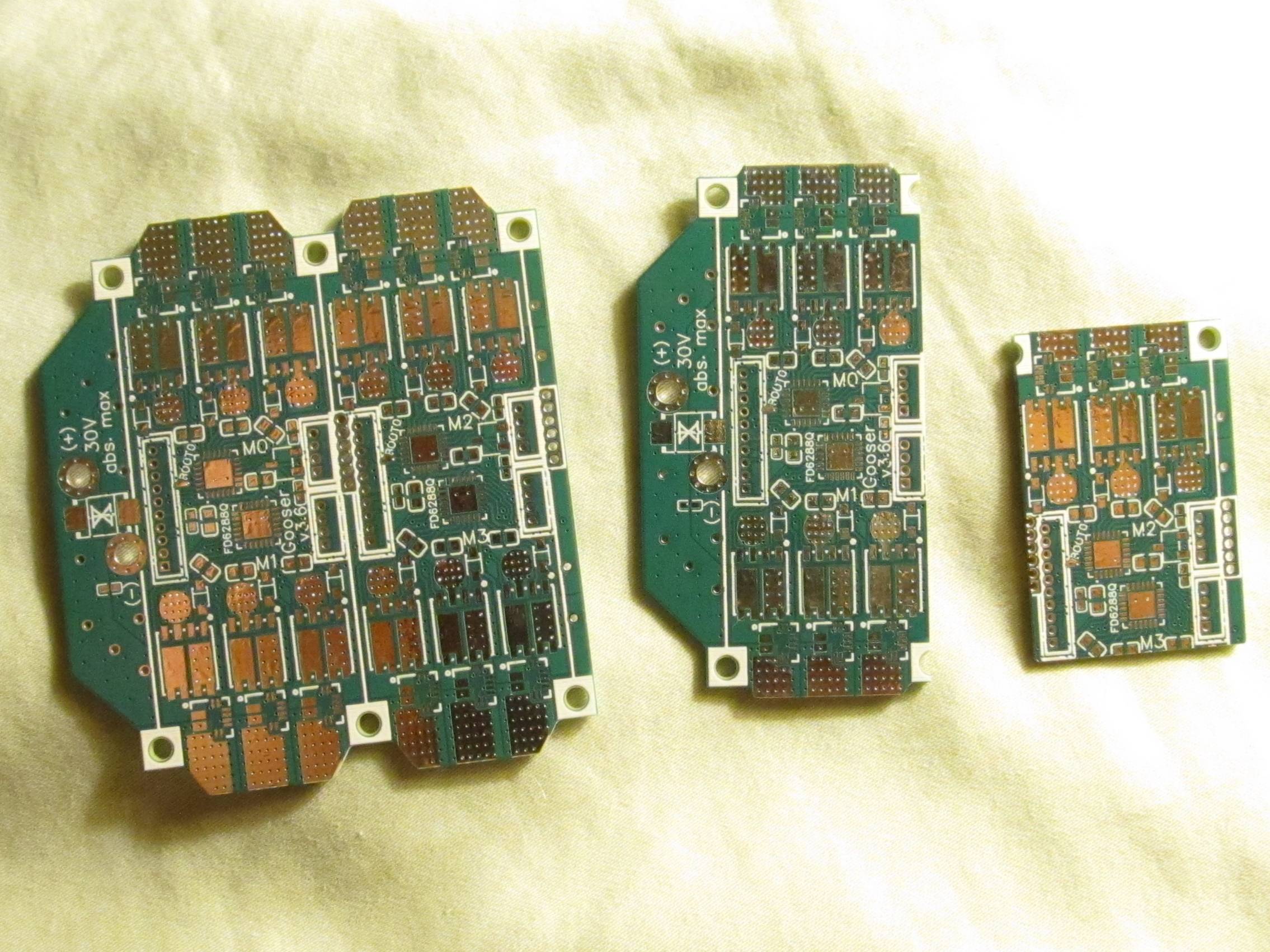
The order is in! A mere $9.50 for 5 boards shipped, thanks to a $5 coupon I got from the new points system on OSHWLab. This will allow me to assemble and test a 2-motor board for minimal cost. Depending on how difficult it is, I’ll either do the rest freehand as well, order another 5 plus stencil, or order 5 assembled.
I made one more insignificant change. I didn’t like the encoder connectors being the only points of access to the 3V rail, so the extra holes on the edge of the board are now included on the 2-motor version rather than just my 4-motor variant, and include a 3V hole. It is in a slightly hazardous location since the 3V regulator outputs should not be connected together when stacking boards, but there’s nowhere else for it.
I also made an amusing realization that you can cut off everything south of the programming connector and it will still be totally functional for one motor (20x32mm minimum size, if you use the back side motor wire pads so you can cut 2mm off the top too). And since you don’t need the input terminal area, two of those side-by-side is actually smaller than the intended two-motor version (though they are in series then, but you can solder the input wires along the back to serve as copper bars).
At long last the boards have arrived! With a bonus 6th even though the order was for 5. Is that typical when ordering non-assembled boards?
I discovered one error which limits the maximum voltage to 20V. When I split the driver voltage from the main input, I forgot about the bootstrap diodes, so they are still connected to HV_IN. If DRV8300 will work this time, I can just leave the diodes out. But I’ll fix it in the PCB design later.
I cut one board up into a dual-motor and single-motor format. The dual-motor lost its edge pins and VDRV solder jumper, but is still perfectly usable. The single-motor is currently 21.5x32.5mm but the right side 2mm margin could still be removed, and bottom edge could be shaved a bit closer to the capacitor which is the southernmost essential component. I would have preferred to keep the left side 0.5mm wider, but I prioritized the dual-motor since both have traces near the cut line. It was a close call on the top left diode’s VDRV HV_IN line, but it is intact.
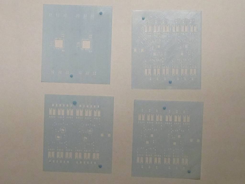
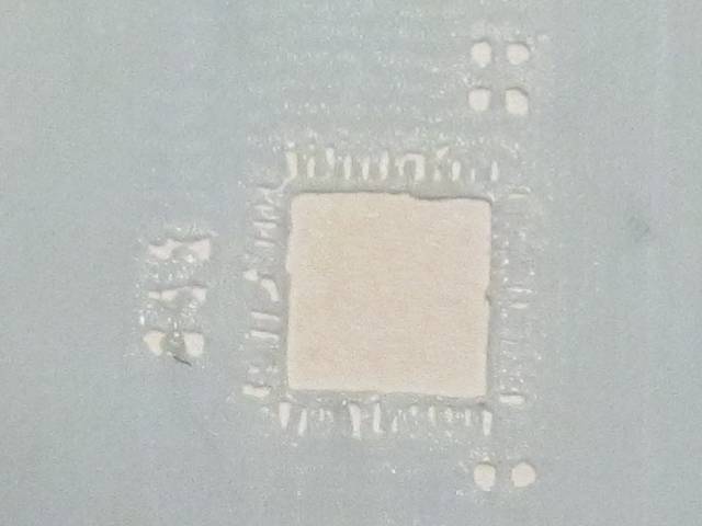
I tried to 3D print some solder stencils with a 0.2mm nozzle, but I don’t think they’ll be usable. I do think the machine is capable, but it’s hard to wrestle the slicer into doing exactly what I want. I may try writing my own g-code generator.
I could also try CNC milling, but it might get expensive breaking 0.3mm drills and end mills, plus I’m not sure how to hold a 0.1mm thick sheet of metal. Masking tape and superglue seems the only way, but then how to peel it up at the end without bending it? I could use plastic, but that needs downcut and 0.5mm is the smallest end mill I could find. No good for 0.5mm pitch pins.