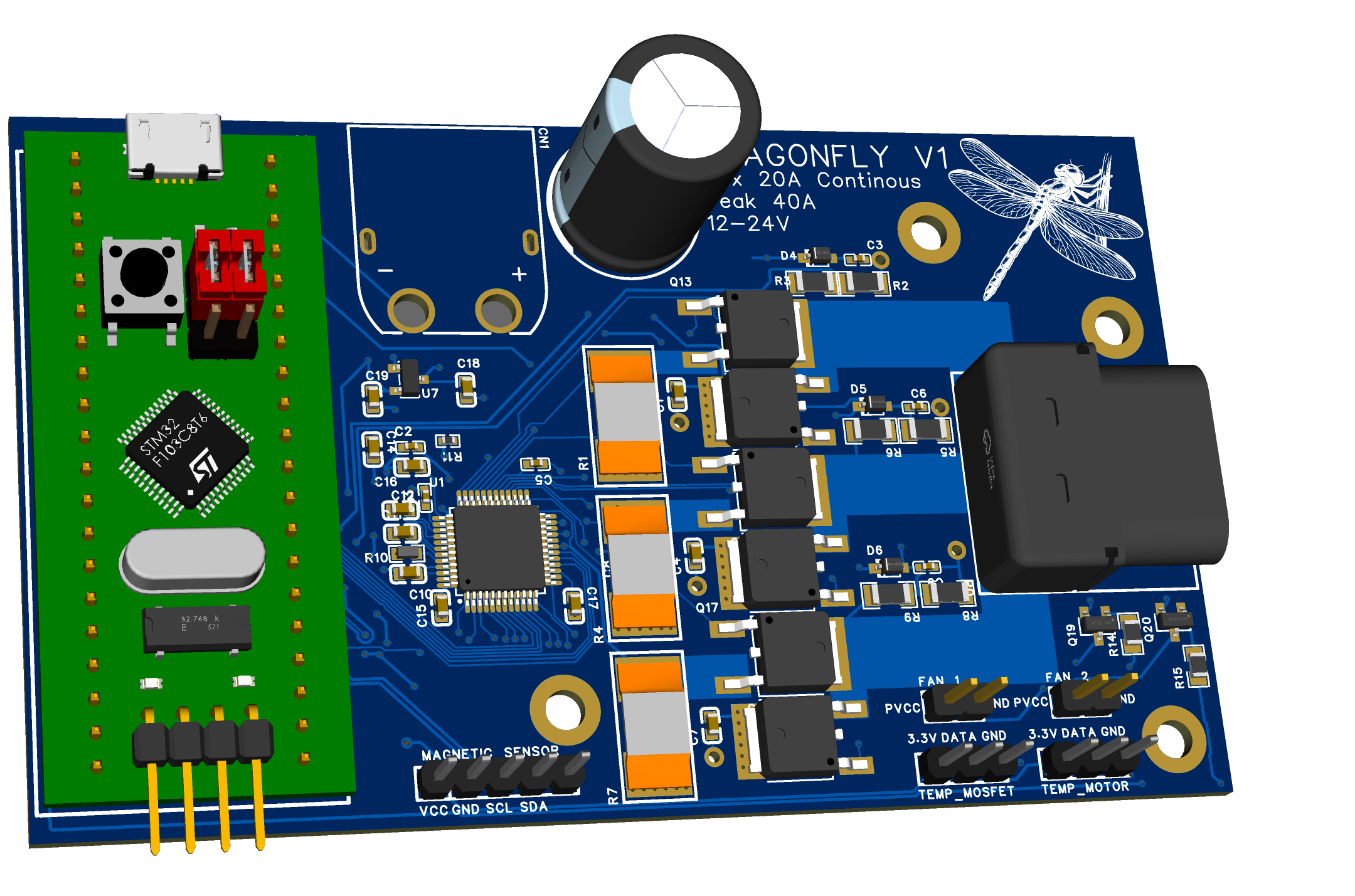
Hello everyone, Ive been designing a custom driver board for a robot arm recently and id like to ask the smarter than me people here if you could take a look at it before i commit to an expensive order. Its my first time doing such complicated electronics and its rather expected for me to have made some boneheaded mistakes.
Built with the bluepill microcontroller and drv8305.
Its specs are 20amps continous, 12 or 24V, low side current sense and voltage sense, and connectors for two temp sensor and associated cooling fans. With the intent to drive a cheap 5010 motor in position control mode.
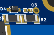
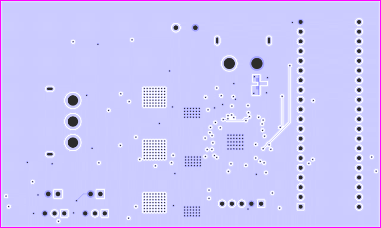
Most of your mosfet vias are being wasted by the thermal reliefs on the inner layers. Only the outermost vias are actually connected to the power planes. Put solid rectangles over them to fix it without having to turn off thermal reliefs for the pin pads.
With the exception of differential pairs, traces should generally be spread apart from eachother rather than bunched as close as possible like you have them. When they run close together for a long distance, they function as a capacitor and induce currents in eachother (called crosstalk) which can cause problems. Especially if it’s a digital line running alongside an analog line, e.g. the line running from a current sensor to ADC pin. Give analog lines as much space as you can.
While it is nice to have all the routing on the outer layers so you can visually follow all the connections, I’d recommend ground on inner1, routing on inner2, and positive plane on bottom. For one thing, the outer copper is twice as thick as the inner so it’s a waste not to use it for at least one of the high current paths. But more importantly it should reduce noise/EMI issues since both routing layers can use inner1 for their return currents. But since both layers’ return currents will be running in the same ground copper, they will still contaminate eachother. So try to space lines apart from eachother on both routing layers too.
Alternatively you could keep bottom as the second rounting layer and use a technique called coplanar grounding on it, but it’s more difficult and uses more routing space. Put a ground via next to each signal via, and run ground traces alongside each signal trace on the bottom layer. The return current for top layer signals will travel in the inner1 ground plane, then go through the ground via, follow alongside the bottom layer trace, and back through another via to inner1. No shared ground plane, so less crosstalk between return currents.
I wouldn’t necessarily say that’s “it”, just my initial thoughts when looking at it
Can I see the schematic and 3D model view? It looks like you have a capacitor overlapped with the second current sense resistor, but maybe I’m not understanding the footprints correctly.
I’m not particularly knowledgeable about this, but I think current sense resistors need the traces routed from them in a particular way to get good readings. Google “current sense resistor kelvin connection” and read about it.
With this trace, I’m pretty sure that you don’t have pullup resistor for I2C lines.
I’m kinda prefer SIG GND GND SIG for this design. Even though we’ll need high current path, we still able to draw some polygon on the Top & Bot layer for it.
For current sense, you better route it as differrential pair. You can do like this:
In schematic I will use a nettie to actually separate the high current path with sensing net.
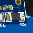
About the copper imbalance, you can route trace for both pads, or you can select the pad on the polygon and edit its property to have thermal relief connection instead of solid
Huh, wouldnt thermal relief connections worsen the conductivity of that path? The whole phase current will be flowing through there when its acting as the low side connection of the motor.
DS8242-33 is an LDO. And you are using it to stepping down from PVCC → VCC. I don’t think it’s a good idea, you should use buck to do it instead.
The VREG pin of DRV8305 is the power output pin. In your case, if you want to use it, then you can ignore the DS8242-33 entirely and power the MCU with it, but it will become chicken-egg problem. Otherwise, you can power it with some buck as I mentioned above, and do NOT connect the VCC to that VREG pin.
Do you have any specific reason why using different component package? If no, please be consistence here, in this case I think choosing 0805 or 0603 is enough, we don’t need to go to 0402
Don’t use pin headers, especially male pin headers with low pin counts. It will come off easily, trust me . You should use more rigid one, eg: XH connectors 2.54mm pitch, or PicoBlade 1.25mm pitch.
Stub detected. You don’t want to build an antenna here, don’t you
Yeah, I know i was just lazy and didnt want to implement a buck, i suppose i really should.
The variant of the drv8305 im using is supposed to not have the internal regulator, as far as im aware.
The reason there is simple, its the first one of that value that came up in the jlcpcb basic parts catalogue. Will see if theres one of a consistent package available.
Ah its even worse than that, i didnt finish connecting vcc to the voltage divider.
The squared resistor is the one that has copper imbalance, so I adding thermal relief on that pad connection to the copper zone to make it balanced again
so about as i thought, and that doesnt hurt current carrying capacity much?
Yes, because let's think about it. Current in = Current out. If we have imbalance copper, it implies that the less copper one already have less current, so it is not hurt at all
Ive been looking at implementing a buck converter and its looking to require quite a few parts that would noticably increase cost of the board with their setup fees, mainly the large capacitors. Why is the LDO such a bad idea? While it would be dropping a lot of voltage the circuit shouldnt draw much current, not even 3 digits of mA i dont think.
You could copy the low voltage buck from my Gooser4. It only uses two extended parts (the nearby TVS diode SMM4F26A is not part of the buck converter). It was designed by @Valentine on his Mosquito, and I’ve rearranged it a bit and reconfigured to output 4.3V which I then regulate down to 3.3V for maximum stability. Mosquito has it output 3.3V and uses that directly, which would probably be fine for you as well since you’re not using 3.3V analog sensors. Replace R1 with 33k to output 3.3V. EDIT: On second thought, the bluepill has a regulator onboard, so stick with the 4.3V.
Unfortunately Valentine has taken his designs offline for the time being, but hopefully he doesn’t mind me sharing fragments of them I copied in the past.
Regulating 24V to 3.3V would be wasteful, but I think it would work. I’m not sure about F103, but STM32G431 uses around 35mA, which is 21.7V*35mA=76mW of heat. The bluepill board has some LEDs that will use more, but the datasheet says that regulator can survive 500mW so you should be ok, especially with a fan blowing on it. EDIT: Calculation error. It’s 760mW, not 76. The regulator will burn up.
P.S. I’d stick with JLC basic parts for the capacitors rather than trying to ensure that they all use the same package size. Larger packages are easier to handle for manual assembly, but irrelevant if JLC is doing it, and extended parts fees add up fast.
Good suggestion with the Mosquito regulator. But with the math looking like what it is i think ill stick to the linear regulator, and put it a connector for an external buck regulator for when that doesnt suffice, the onboard regulator is only really for temporary testing setups anyway, as anything permanent is gonna need its own beefy 3.3v power this can tap into.
Gave as much space to each trace and component as i could.
Implemented diffrential pairs for the current sensing, though with some of those runs being so short theres not much of that.
a little extra cooling for the linear regulator.
Not gonna have the pin headers assembled by the fab, instead gonna solder in whatever 2.54mm pitch connector is appropiorate at the moment, so a jst for permanent mounting and pin headers for testing.
Still using the ds18b20 thermal sensor as it might not even be necessary for the mosfets and its not really worth the board complexity to add a pcb mount one, also - laziness.
Definitely not perfect, but nothing ever is and it should work nicely. As long as i didnt miss anything, which judging by the previous design i probably did.
As said earlier, I’d recommend ground on inner1 and positive on bottom.
If I understood all those Robert Feranec videos correctly, it’s possible to use the positive plane for return currents, but only if the signal originates from the same voltage. I think the DRV’s internal regulator would qualify as creating a new voltage origin, so the signal lines going to the MCU will have their field spread out to reach the bottom ground layer, polluting nearby traces on both routing layers. Whatever DRV8305 does to step the input voltage down to 10V for the mosfet gates probably qualifies as a new voltage origin too.
They all have a shared ground voltage, so using it is the most reliable way to keep the fields compact. And putting it between the two routing layers means you can via between them without changing reference plane, so you don’t need ground vias all over the place.
But now that I think about it, with inner2 being between the power planes, traces on it could get polluted by the high power current if they cross through the area between the input connector and mosfets. Maybe the coplanar grounding strategy would be worth the effort after all… though if you’re tired of working on it, just go with inner1 ground. All this careful waveguide crafting is a fun game for me, but EMI is usually not that big a problem anyway.
Overall it looks fine to me. The traces could use a little more massaging to eliminate sharp corners and pointless squiggles, but I doubt those would hurt anything anyway.
Alright then, a few slight fixes and it should be ready
Tired isnt the word id use, but yeah, it only needs to be so good and worrying about EMI and similar things probably isnt worth it compared to putting that time into other parts of the project. Thats something i can learn when I inevitably have to design RF stuff.
All digital circuits are RF. The sharp transitions create a pulse of high frequency energy.


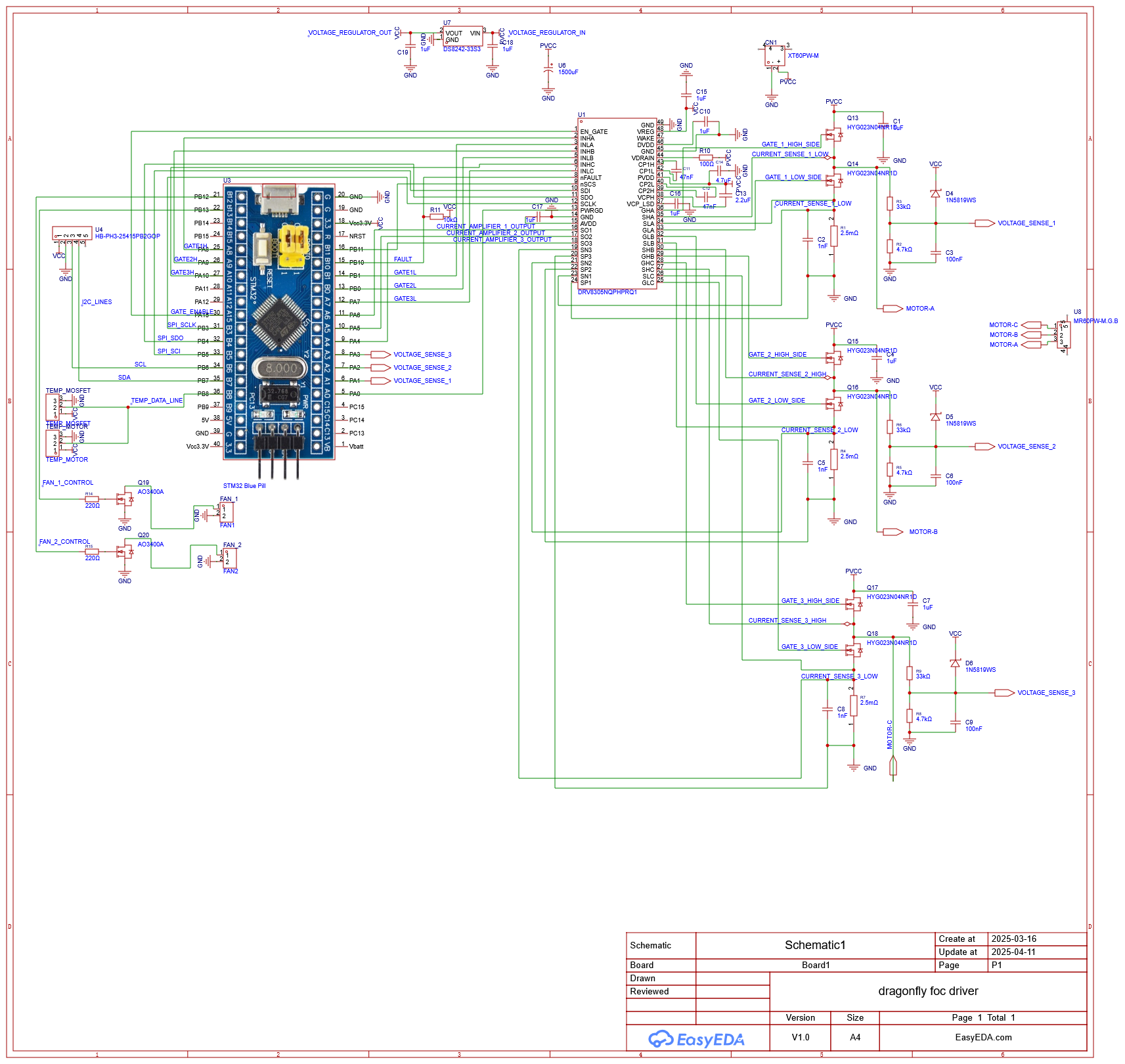


Arggggg!!! Net labels net labels please.....
– RikkyThe joys of beginners designs, ill add those and reupload the schematic
– kamilo154Done, if somethings still unclear or hard to see lemme know
– kamilo154About the copper imbalance, you can route trace for both pads, or you can select the pad on the polygon and edit its property to have thermal relief connection instead of solid
– RikkyHuh, wouldnt thermal relief connections worsen the conductivity of that path? The whole phase current will be flowing through there when its acting as the low side connection of the motor.
– kamilo154