I didn’t find good low priced options for 48v boards so started to work on my own to make use of mass produced 48v bicycle/scooter/skate hub motors and battery packs. These are the first boards I am building and I started with the open source trinamic kicad files. I am trying to select chips that have good availability.
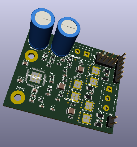
One gate driver board is using the TMC6200 60V with inline current sense. It has a limit of 10A when using the built in current sensing. goal is mid power with high efficiency.
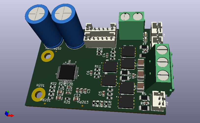
The other gate driver board is using TMC6100 60V with low side current sensing (3x INA180A3IDBVR). That will be a higher power board such as 20-30 amps continuous.
Current plan is to use jlcpcb with the smt process and then add the TMC chip with a small solder mask and then reflow the board.
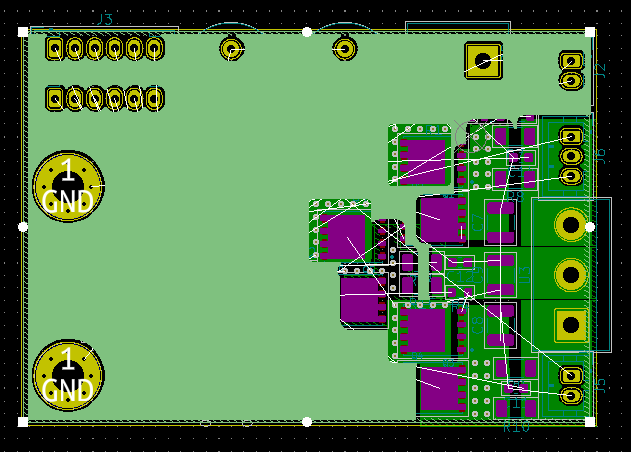
Made some progress on the board and panelization. Trying to fit 24 panels into a 250x250 limit for jlcpcb smt process. kikit was used for automated panelization.
looking at the 3D-render, it’s a bit hard to see from the angle… Does a heat-sink fit over the FETs? It looks like that if it weren’t for the white 6-pin connector, it would be possible to put a heat-sink across all the FETs, but as it is the connector might be in the way.
This, and the output capacitors are higher, and no heatsink bolt-holes so unless the radiator is milled to spec and permanently glued with silicone it won’t be an option. These mosfets will get really hot. I’m not criticizing the design, may be there are things I don’t see.
I am thinking about using 30x30x20 mm heatsink with 2 push pins both with fan and without. Internal push pins are not working but I think I could get tabbed push pins to fit.
I did modify the jst connectors so that the heatsink will fit over all the mosfets. I was able to add .5 mm to the board width and still come under the 250 mm for 6 boards.
Third image is the heatsink with internal push pins that I dont think I can fit so now looking at tabbed push pins.
I’m not giving you design advise, just off-hand comments. In these cases perhaps silicone glue would be best, avoid any mechanical fastenings. High-temperature resistant and flexible.
1oz copper could be improved if you add rails/bus bars but that would require bare copper and post-processing, not out of box. Another option is 4 layers and use vias to increase the copper cross-section and use separate planes for power and ground on the power side, that would make 3oz (1+1+0.5+0.5) copper. This is the only way you could pull 30A before the solder melts and mosfets pop. This, or go for larger mosfets where you got more copper area underneath.
I’m posting here because I am hoping for comments on issues with the design so thanks for the feedback. Design goal is to make a quality open board at lowest possible price + lowest manual labor for post process and testing.
I am planning on using 4 layer boards since it only adds .20 to the panelized board cost. I will look into the 3oz (1+1+0.5+0.5) copper technique.
I’ve noticed the high current boards are difficult to produce at a low cost because of the manual steps and testing needed after the smt process. For example, soldering the leads directly to the board instead of using a terminal block or adding busbars/heatsinks/fans.
The <10Amp board BOM cost is 8 euro + .70 for the 28x28x20 heatsink. Manuel step of adding the gate driver to the board and maybe gluing on the heat sink. So total bom of 8.70 euro priced at quantity of 120.
The higher amp board BOM cost is 10 euro, .5 for 28x28x13 heatsink and 3 euro for 3010 sunon fan. Manuel step of adding the gate driver to the board and maybe gluing on the heat sink/attaching fan to heat sink. Then direct solder of 12awg leads to power and motor terminals. Copper pcb rivets on the 5 high current terminals might help. total bom of about 15 euro priced was priced at quantity of 120.
Seems you have the issues well under control. If you have really pointed design questions, please ask.
That’s pretty incredible. I’m quite happy if my boards are <100. My Jackhammer when fully developed will be around $100 for a small batch. Seven high quality, production grade mosfets are $8 each alone, that’s already almost $60 excluding design and engineering and testing and whatever else comes after that.
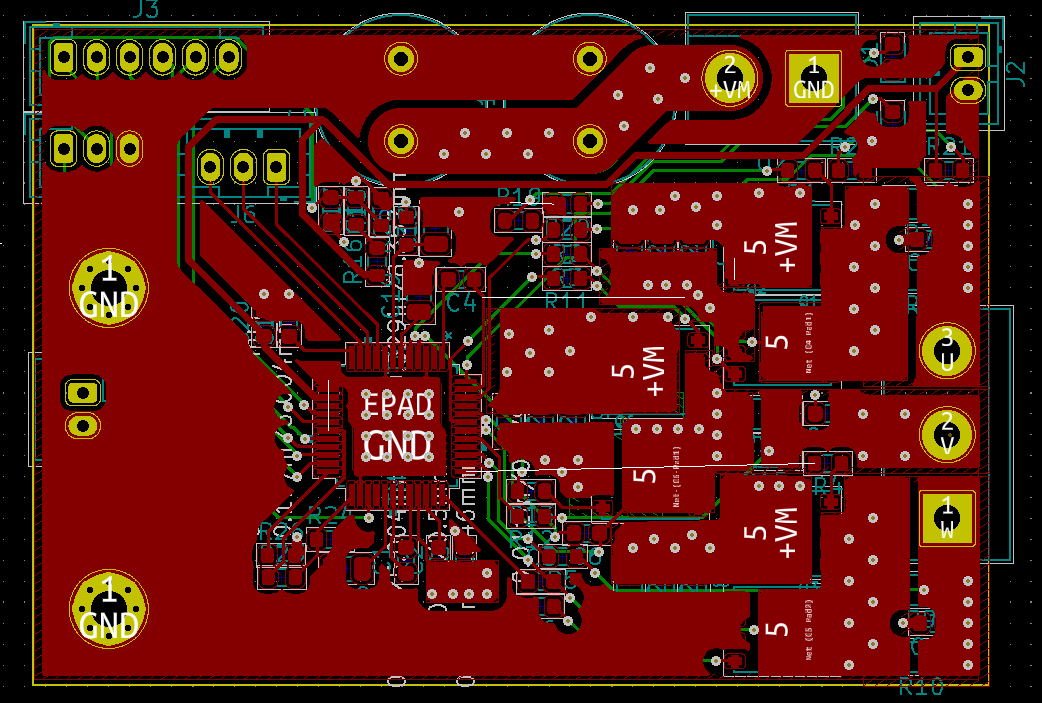
Something else you may wish to consider. JLC allows you to have exposed copper areas. When you expose the copper area, they bathe it in tin, thus effectively increasing the thickness of the copper. Also you may post-process the exposed areas and manually thicken it or solder a bus wire. This is the top and bottom of my most recent board, pay attention to the exposed copper areas.
I have started routing traces now. One layer will be a +VM copper pour. I wonder if there is an issue having that on the back 1oz layer?
Then I did pours for the high current areas on the top and bottom layers connected by vias.
The big capacitors are using 1+.5+.5+1 = 3 oz copper. The 4mm trace has about a 25 celcius temperature raise with 10 amps. (Needs more vias still)
Finally I am planning on using the autorouter to finish signals on 3 layers and then do ground copper pours over those. I already did many iterations with the autorouter which found some issues.
Moved bootstrap capacitors back behind the mosfet pair. I parallelized them with 3x 0805 1uF capacitors to keep them at the same height as the other components I will put the heat sink over.
started manually routed trace. Those on the upper left I will likely put to the back of the board or there will be no space for future component additions.
added a fan jst connector (j4). though it is not wired up. Was thinking to send the temperature to the controller that can decide whether to turn on the fan + have some temperature the fan comes on automatically.
TMC6100/TMC6200 can use SPI pins for configuration instead of SPI. If you don’t do this your controller will need to use spi to set parameters at power up. That is a special knowledge I don’t want the controllers to need to have. So far I have disabled spi in favor of using the pins for configuration.
Thinking about adding sleep circuit but this again causes special knowledge in the controller so will skip it for v1.
Next Steps:
Now thinking about changing from 0603 to 0402 for the basic resistors and capacitors. I am making other boards (mptt and bms) that might need the smaller parts and want to use consistent parts across all of them. The ability to repair is already impaired if I glue a heat sink over the majority of components.
might parallelize some other capacitors for increased reliability.
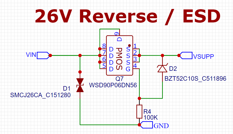
You may not have space for reverse polarity unless you seriously rearrange the routing, capacitors, and remove the two GND mounting holes. If I were you, I’d also add ESD/overvoltage protection on the power inputs. The way your power comes from the side, you need to route the power to the butt of the board where the free space is for these, it’s going to be very hairy, since you will cross the signal plane.
That’s a lot of components up there, and at that voltage and current they are pretty big. You must change of course the SMCJ to match your voltage limit. 26V may be a bit too low for you.
Also, for the fan controller, just give users a 5V-GND pins to attach a fan, no need for an active fan controller. Any cheap small 5V fan for RPi will already have a variable speed fan controller inside, you may want to expose the speed pin, too.
Also the driver is out of stock, how do you do this?