Finished the layout, it’s a 4 layer board with SIG/PWR, GND, GND, SIG/PWR. Doubting about the current sensing part and the PWM traces.
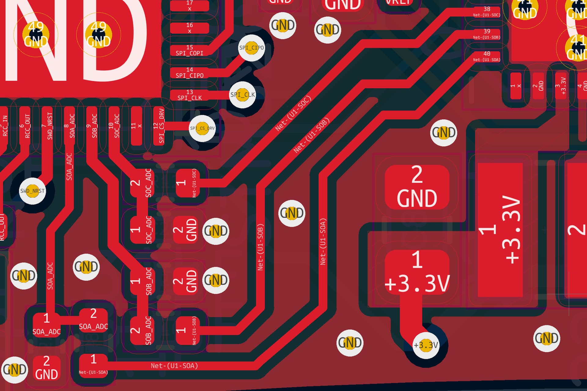
The A/B/C current sense traces go through a 1k resistor and 30pF capacitor close to the STM32. The layer below is fully poured with GND. Bottom right are the inductor and capacitor of the buck.
Here are the 6x PWM traces.
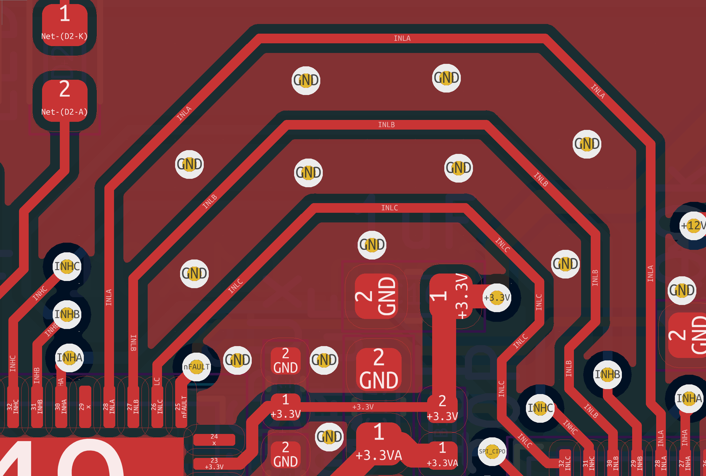
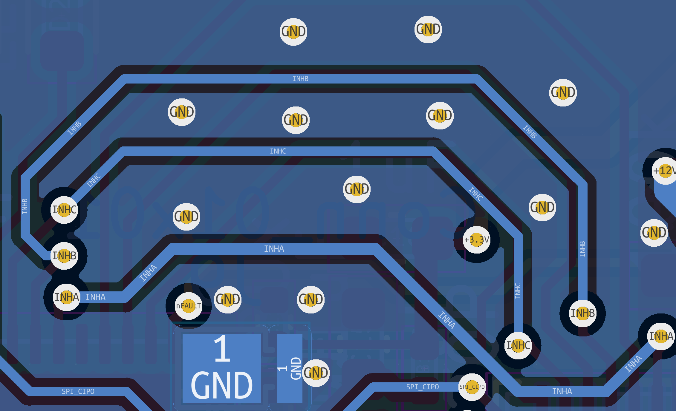
Since the timer pins of the STM32 don’t match the order of the DRV8316C I had to route them to the 4th layer and back. Will this cause any issues?