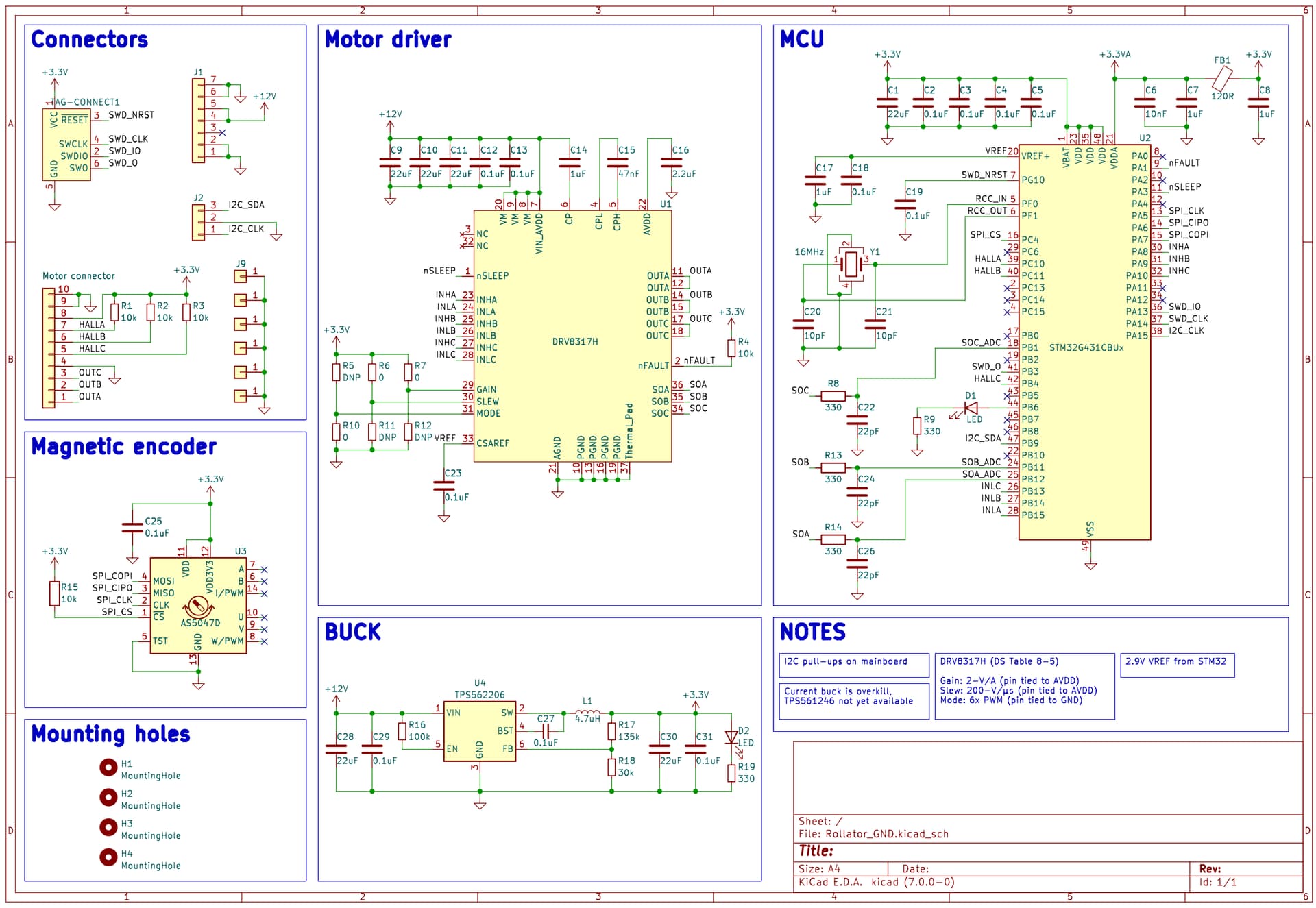
I’ve been through most of the schematic review topics here, which have been very helpful. Before proceeding to the PCB design, I’d appreciate if someone could review my schematic. The main components are an STM32G431CBUx, TI DRV8317H, and AS5047D magnetic encoder. The motor itself is a 12V, max 1.3A (stall current) BLDC motor with hall sensor feedback.
I’ve had a quick look at your schematic, and I cannot see any major issues. I have a few suggestions which may improve your design.
If you think the buck converter is overkill, you can use the DRV8316 which is very similar to the DRV8317, supports more voltage and current, and has an integrated buck converter up to 200mA. Alternatively, if you don’t mind lower efficiency, you can use the integrated 3.3V LDO (on AVDD) to power the microcontroller, which supports up to 80mA. STM32 uses 65mA under worst case scenario with all peripherals enabled, and encoder uses 15mA worse case, so you have just enough power.
Consider connecting the incremental encoder interface (ABI) to your microcontroller as well, the incremental encoder interface is much lower latency and it will perform much better than reading the angles from SPI. The datasheet says the latency of SPI readings is around 100us, while it is 2us on the ABI interface after angle error correction.
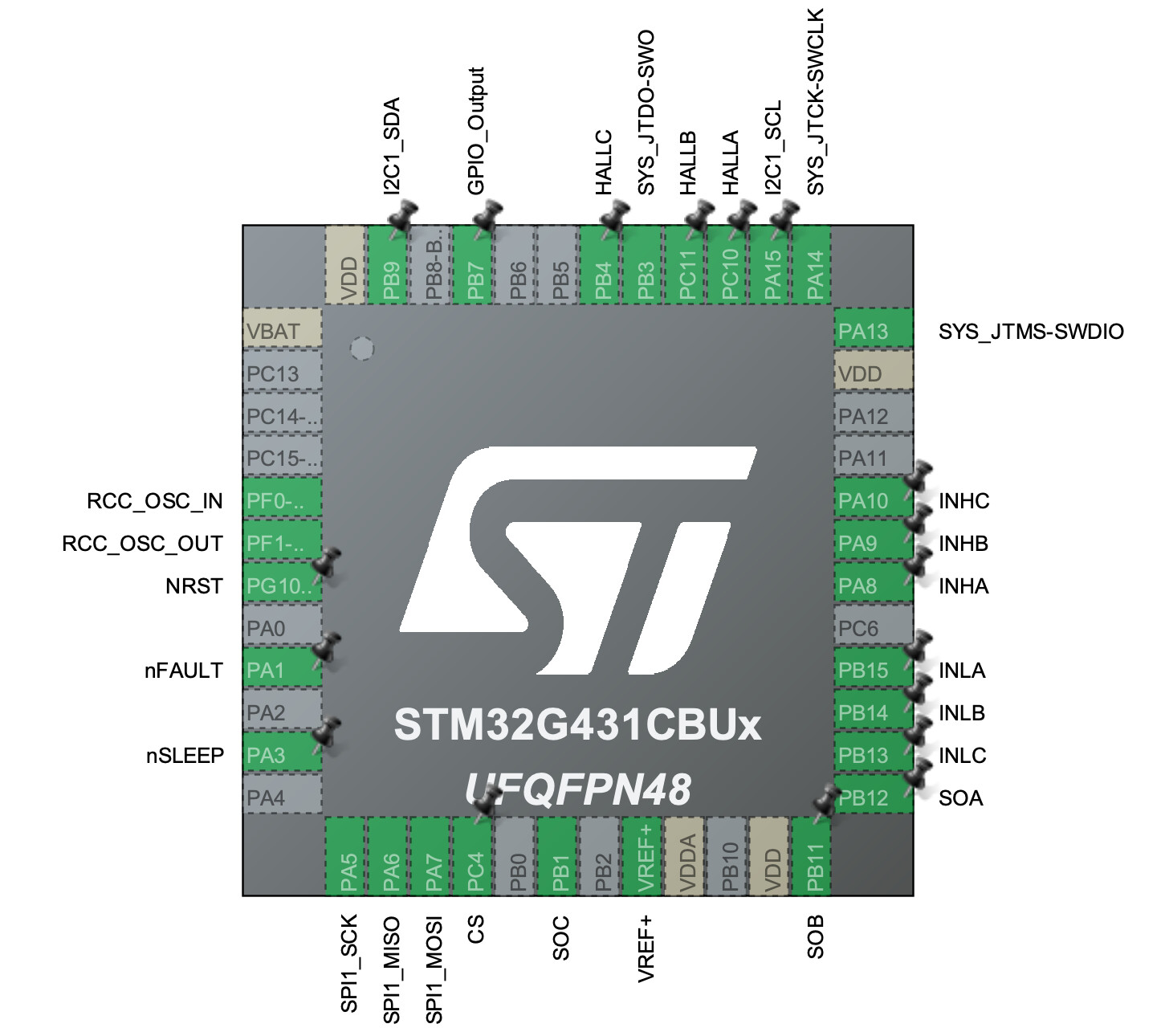
Consider changing the ADC pins used on the microcontroller to favor lower ADC channel numbers. This is because the lower channel numbers are “fast channels” and have slightly better performance. I suggest pins PA0, PA1, PA2.
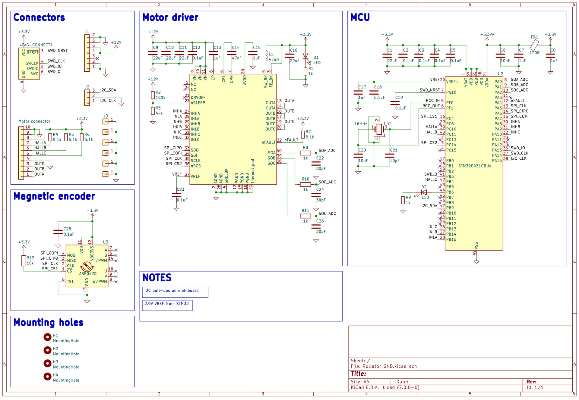
Great feedback Andrew, thank you. You convinced me to switch to the DRV8316C, it’s a bit more expensive but the integrated buck makes up for it. Do you recommend placing an LDO after the buck to reduce ripple? I see the buck voltage can be set to 4V for this. I’m mostly concerned about the STM VREF stability which is used for the current sensing. In STM’s AN5690 they mention that VREF is “is based on a low‑drop output regulator design”, so maybe another LDO is overkill.
The encoder is tracking a very slow rotating pulley (<100rpm), so the 100 µs is more than enough. Thank you for the suggesting though. I’ll be changing the ADC pins to your suggested pins. Thanks again
I agree strongly with this, especially as you have lots of spare pins… connect A and B to channels 1 & 2 of a general purpose time to use the encoder mode.
Updated schematic with DRV8316C. Due to the integrated buck requiring nSLEEP to be pulled high, it is always driven high by the voltage divider. Should there be a small 0.1uF capacitor here to stabilize the voltage?
Your design looks fine as is, I wouldn’t recommend an additional LDO after the buck as digital circuitry is not noise sensitive, and you already have a filter for the analog supply, which is going to be good enough.
In my design using the DRV8316, I used the internal AVDD LDO directly as analog supply voltage and reference voltage, as I wanted a 3.3V reference voltage, however I think your approach is better as it is higher efficiency.
You can consider replacing R3 with a 3.3V zener diode, so you can get a wider range of operating voltages. A capacitor is unnecessary here.
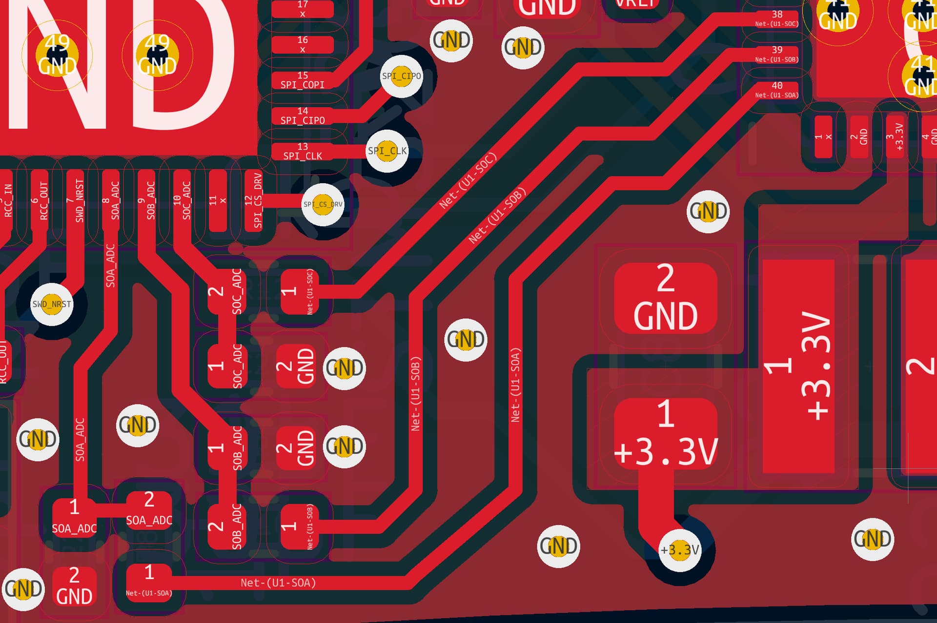
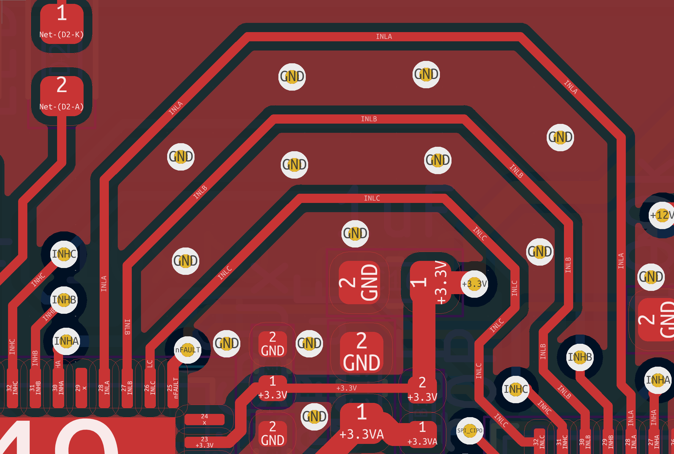
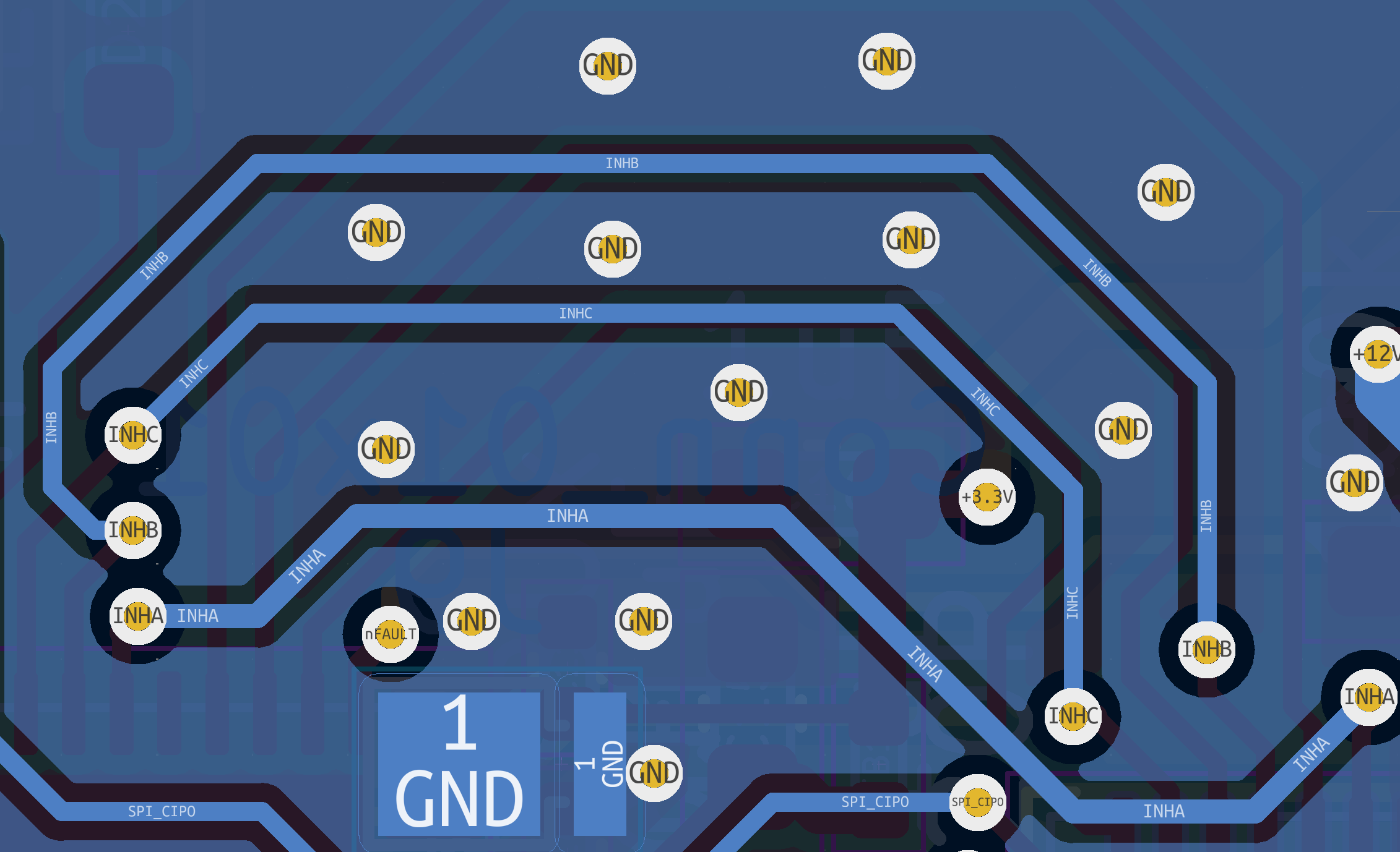
The A/B/C current sense traces go through a 1k resistor and 30pF capacitor close to the STM32. The layer below is fully poured with GND. Bottom right are the inductor and capacitor of the buck.
The current sensing traces are probably fine, although the component values are slightly off from datasheet recommendations.
You might want to check your schematic for the PWM pins as I think the order of some of them might be swapped. Also there is no need to put GND between the PWM traces, just route them next to each other to save space.
Your PWM pins configuration in STM32CUBEMX looks fine, and when using 6x PWM you have to make sure the CHx needs to be connected to INHy and CHxN needs to be connected to INLy. Currently you have them swapped on the STM32 side. Connecting CH1 to INHA, and CH1N to INLA is one way to do it.