Hi everyone,
I am working on a 3-DOF attitude control system for a satellite simulator using three B-G431B-ESC1 ESC boards driving Sunnysky V4008 380KV BLDC reaction wheels. I have removed the daughterboard (in hindsight highkey a mistake on my part i admit) and need to program the STM32G431CB via the J4 SWD pads using an ST-LINK V2.
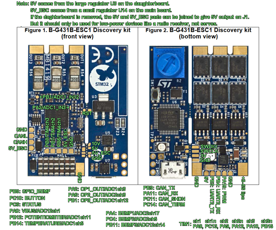
My question is about the J4 pad orientation on the bottom side of the board. The manual confirms the 4 pads are:
Pad 1 = SWDIO
Pad 2 = SWCLK
Pad 3 = MCU VDD (3.3V)
Pad 4 = GND
However I cannot clearly identify which physical end of the 4 pads is pad 1. A photo or description of what to look for would be greatly appreciated.
I am using SimpleFOC with Arduino IDE and the B-G431B-ESC1 board definition. I just need to confirm pad numbering direction before I solder so I do not damage the board.
Here’s my cheat sheet, made by probing the CPU pins to be sure which is which.
EDIT: Updated image with two more pins. Turns out TP3 and the little solder pad to the upper right of the CPU are both ADC pins, which means the LinearHall class is usable on the ESC1.
THANK YOU SO MUCHHHH THIS HELPS TONSSS T_T
I was genuinely losing my mind over this bless youu
You have my well wishes always~ may your solder joints be shiny, your GPIO pins never fry, and your code compile on the first tryy always
Be careful, in my case hall signal pins appeared to be swapped. 5V&GND are correct, but other aren’t. The order is: PB6, PB7, PB8, 5V_ESC, GND from left to right
Indeed you are correct! Thanks for pointing it out.
Unfortunately that post is too old to edit anymore, so here is the corrected version, which also includes two somewhat-accessible ADC pins I found a while back, and corrected the daghterboard typo Hopefully there are no other errors.
 Hopefully there are no other errors.