Yeah, that’s the most common approach I’ve seen for closed-loop on 3D printers. But that locks you into a particular motor form-factor, whereas I’d like it to be usable on as many different motors as possible so people can play with new designs.
If anyone else wants to try a slightly less cramped version, I’d suggest designing for the BigTreeTech EZ slot mentioned in my previous post. Then at least you can buy motherboards to use it directly, and they already sell adapters.
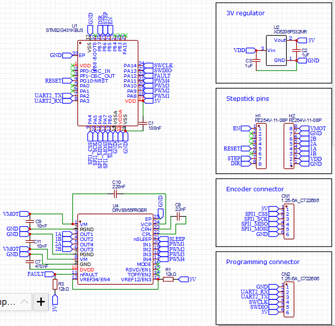
Here’s my first attempt at routing with STM32G431 and DRV8844. The reset and sleep pins were a lost cause, so it will be possible to brick the MCU if you flash a bad firmware and need hardware reset. At best I could make a tiny exposed copper area next to the chip where you could manually operate it.
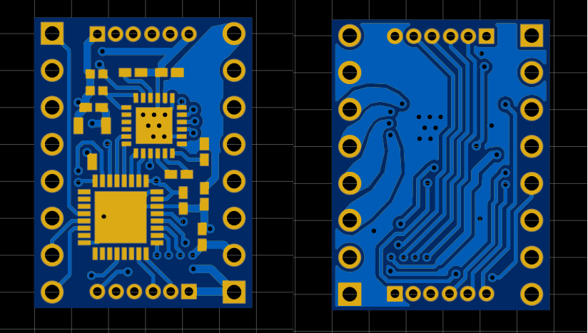
It ended up being better to have JLC assemble the bottom layer, and manually solder just the MCU on the top. There’s also a capacitor for the DRV’s internal 3V regulator that I had to put on the top layer, but I don’t think it’s needed anyway since the regulator output is not used.
There’s one potentially fatal problem, that I had to squeeze the “enable” trace inbetween the DRV’s thermal pad and pins. There’s not quite enough space as-is, but it may be possible to reduce the size of the solder pad on the PCB and count on the solder mask to make sure no solder connects the trace to the pad on the chip.
Otherwise I think everything is good. Power traces are not as fat as I’d like, but not too wimpy. I also wish I could fit one than one via per line.
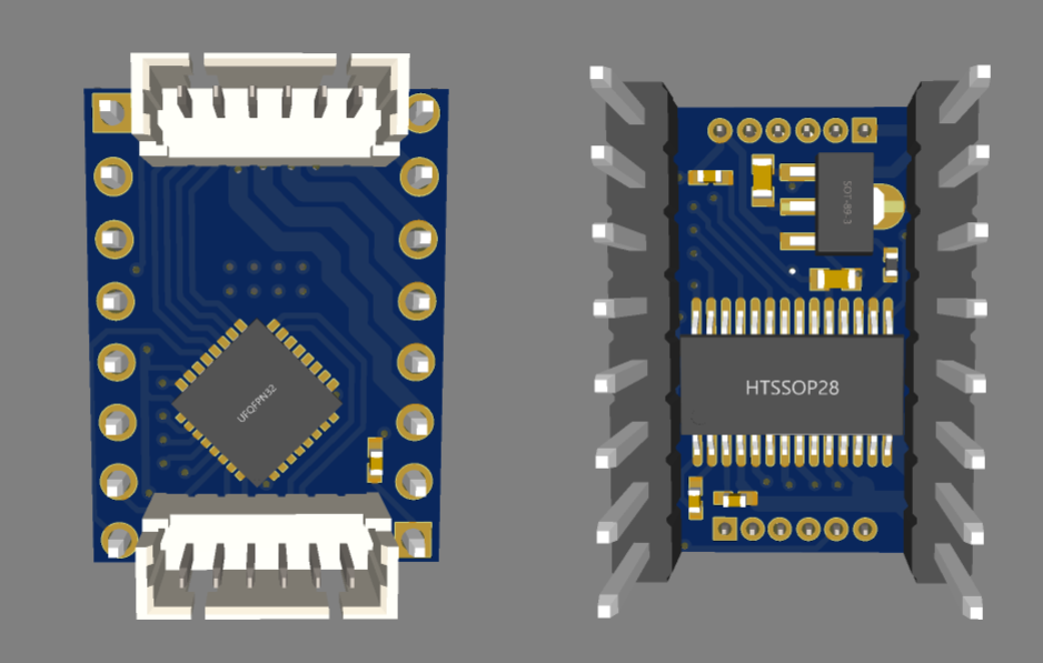

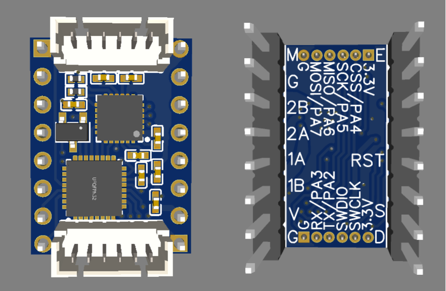
EDIT: Second attempt, using DRV8955. This one is much better. Ready for showtime, I think. Fatter power traces, all components on one side (although the driver will still have to be manually soldered since JLC doesn’t carry it), reset pin connected, and no sketchy practices like routing along the outer edges of the board. I even got the driver fault pin readable by the CPU, though it’s not really necessary. The enable pin goes to the CPU, and then CPU will be responsible for activating the sleep pin on the driver.
One thing that really helped is that I found a smaller voltage regulator on the JLC basic parts page, which also uses smaller filtering capacitors. Maximum input is 6V, but I think the VDD pin should always be 3.3V or 5V. The VDD-to-GND filter cap is father from the regulator than I’d like, but hopefully it will be ok.