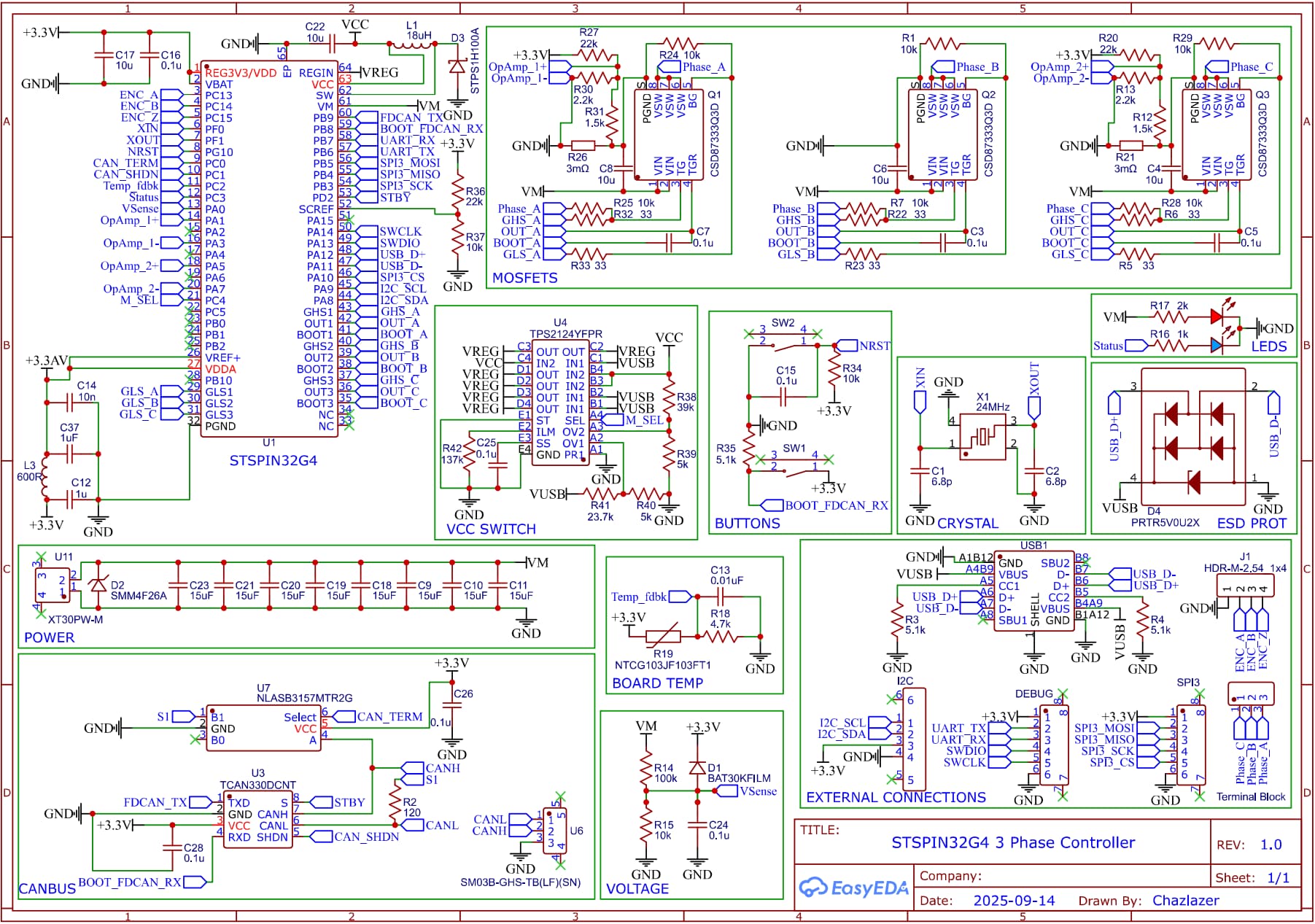
I’m still very new to making circuit boards and still very much a beginner, but I wanted to make my own driver board for an upcoming motor project. I was wondering if there is anything majorly wrong with my current schematic or other things I can improve on and make better?
I plan to use the Stspin32g4 with the internal opamps for current sensing and these CSD87333Q3D mosfets at 24V vm.
Was also wondering if these parts are too marginal at 8V switch driving?
Also TI recommends putting capacitors between pgnd and vm near the mosfets. I think this is for the very high switching speeds? I don’t think i’ll need to go past 40-50khz. I’m not sure if I need to keep these there.
these look like very nice half bridges, with a threshold voltage of only 0.9V, and the Datasheet shows typical values for 4.5V drive voltage. So I would say that 8V is perhaps even a little excessive. I see you have 33Ohm gate resistance, I assume you calculated this?
Consider using 6 single-channel mosfets. They’re available down to around 1.5mOhm RDSon, so for a little more board size you can have close to 3x the power. Otherwise I think the PCB will be pretty large for the power level. I’ve tried designing for STSpin a few times, and all the support components end up taking an annoying amount of space so I go back to my usual G431 and DRV8300.
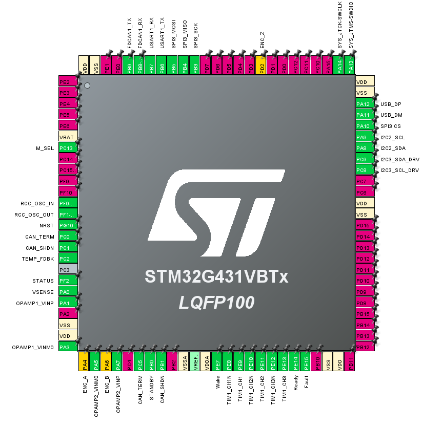
The encoder pins should be three channels of a timer so you can use the STM32HWEncoder class. If possible, make at least two of them ADC pins so it can use linear hall sensors too. PA4, PA6, PB0, PB1 are all TIM3 and ADC. Or PA0, PA2, PB10 are all TIM2, and two are ADC. And shouldn’t the encoder connector have a voltage supply pin?
How did you decide on the amount of bulk capacitance to include? 8x15uF seems very small, especially considering that the capacitance of ceramics is actually much lower than the face value once you apply a voltage to them. Even the 15x15uF on B-G431B-ESC1 seems small to me, but I’ve never known how to calculate the proper amount so I go for overkill.
Thanks. I haven’t actually used the hardware encoder counting, and didn’t realize it has to be specifically channels 1 and 2.
It doesn’t look like there’s any good complete set of ch1, ch2 and ETR for TIM2 or TIM3, but I think it should be ok without the ETR. Section 29.4.22 on page 1304 of RM0440 sounds like you can use it to automatically reset the counter when the index signal is received, but an interrupt on any GPIO should do the job as well.
So then it looks like the best option is PA4(TIM3_CH2) and PA6(TIM3_CH1). Then I see two good choices for the third pin:
If M_SEL can be moved to a different pin, PC4(TIM3_CH3) will enable hardware counting of digital hall sensors.
PA2 doesn’t do anything for TIM3, but it is ADC1 whereas PA4,PA6,PC4 are all ADC2. So then you can sample two linear halls simultaneously instead of having to do them sequentially. Specifically it will be PA2(ADC1_IN3) and PA4(ADC2_IN17), because PA6 is ADC2_IN3 and you can’t sample the same channel number on both ADC units at the same time.
Thanks for the responses! I do need to change some of the pins around. I tend to make a lot of those changes when routing the traces. I didn’t know about encoder pin restrictions.
Regarding the 8V margin. I think the stspin32g4 can only go down to 8V driving voltage, I did have a feeling it might be a bit overkill for this design, but I’m not sure on other options I have to drive the mosfets at a lower voltage.
I didn’t calculate the gate drive resistors, didn’t know what they were for really and I thought I could reference other schematics.
I found this document from TI explaining it. However, I’m not sure on the implications. From what I was able to understand is that I want to dampen out the ringing frequency of the mosfets?
R_Gi is max 6.8? and C is 662pF from the mosfets datasheet.
With Eq1 and 2, R_GATE = 6.8 - 1/sqrt(L( 662pF))*(L/Q)
Does it come down to picking a Gate Resistor that minimizes the Source Inductance L in this equation?
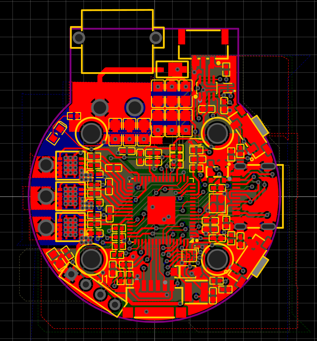
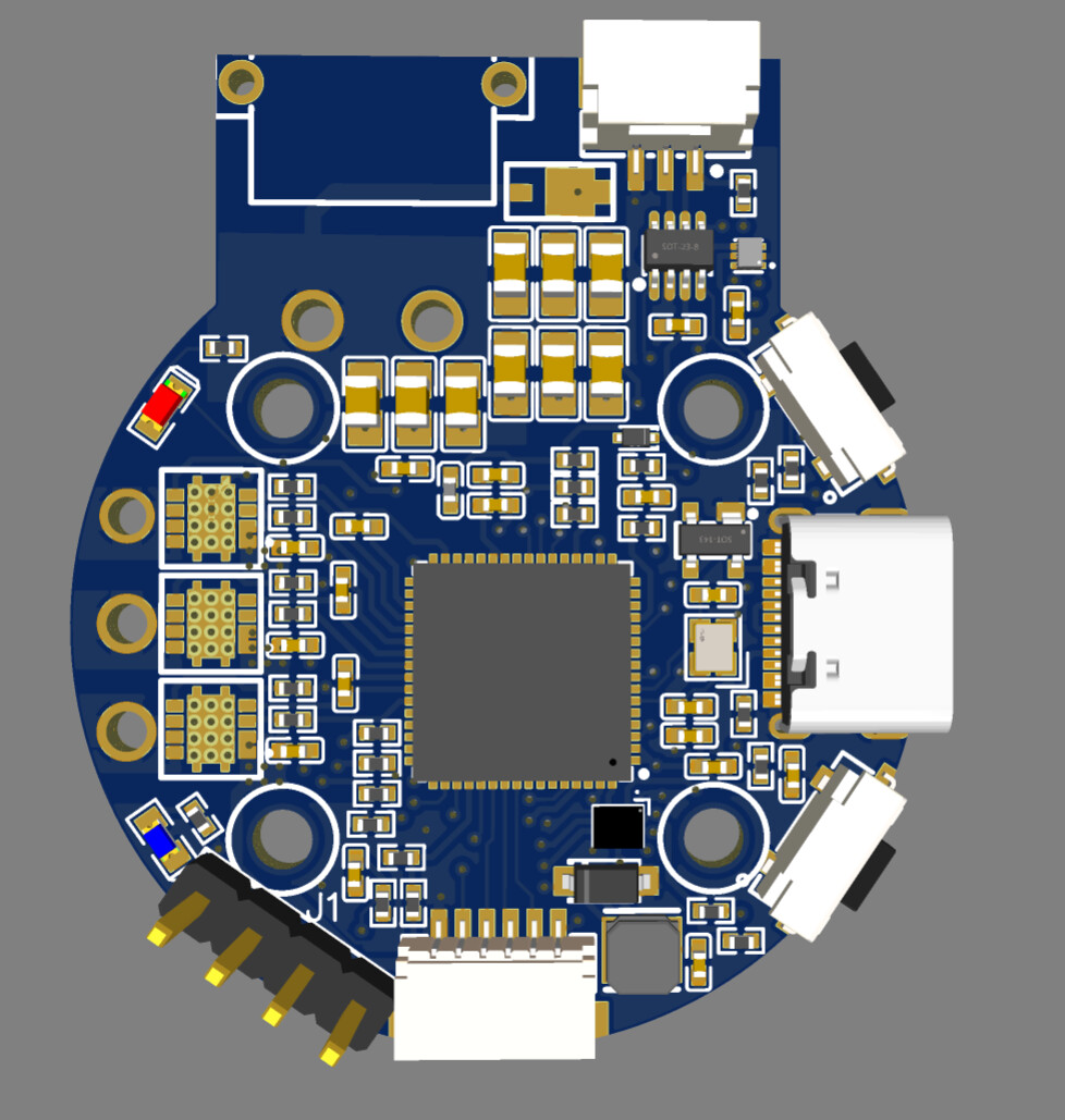
I did consider using 6 individual mosfets and also the beefier cousins of the nexfets, but due to board side constraints I wanted to use these little guys if possible for their size and price. My board is pretty small around 36mm in diameter. I did also find that there is a ton of support components that are needed here and that I had to get rid of the 3rd sense resistor to make room.
I didn’t really calculate for the bus capacitance. If 120uF is too low, ill look into seeing if I can increase it by getting bigger caps. My application is also intended for a maximum of 100 watt motors.
Regarding the HW Encoder pins, In STM MX, I see pins for PA4 and PA6 that they can have their clock source as ETR2. Is this the GPIO for the z pin?
Hmm, I’m looking at the datasheet and don’t see anything about ETR on PA4 and PA6. PA0 and PA5 are TIM2_ETR, but TIM2 isn’t as usable since the only choices for TIM2_CH2 are PA1 and PB3, which are in use by OPAMP1_VINP and SPI1_SCK. You could use PA3 for OPAMP1_VINP and PC5 for OPAMP1_VINM, but the current sense signals should be cleanest if you can route short traces from the resistors to the CPU without any vias, and your original pins are better for that. But if you end up having to use vias anyway, then this would be an option.
There’s also the option of using PD2 for TIM3_ETR, but it’s on the other side of the CPU so the routing clutter will probably be more trouble than it’s worth. But keep it in mind during layout. I don’t even bother making a schematic until the PCB is done and I find out what all pins worked out
P.S. I noticed your OpAmp_2+ and - are reversed (PA5 is OPAMP2_VINM and PA7 is OPAMP2_VINP).
And yes, if you have a hard limit of 36mm diameter, then stick with the small mosfets. You’ll need all the space you can get for capacitors.
The mosfet datasheet shows Vgs=8 giving the lowest RDSon, so I don’t think it’s too high.
My bad, I was wondering if I needed ERT2 as the source for an encoder with an index or z pin. Looks like I do, hopefully the PD2 pin won’t be that bad of a route.
Nice catch! I overlooked the pin numbering, that could’ve been bad lol.
For the Opamp traces, should these be as close as possible to the OpAmp+/- input on the MCU? Unfortunately the Opamp pins seem to be a bit away from the sense resistors, but the support circuitry is close. Trying to get as close to a clean signal as I can with these. Planning for a 4 layer board, I think I can push it to 6 if needed.
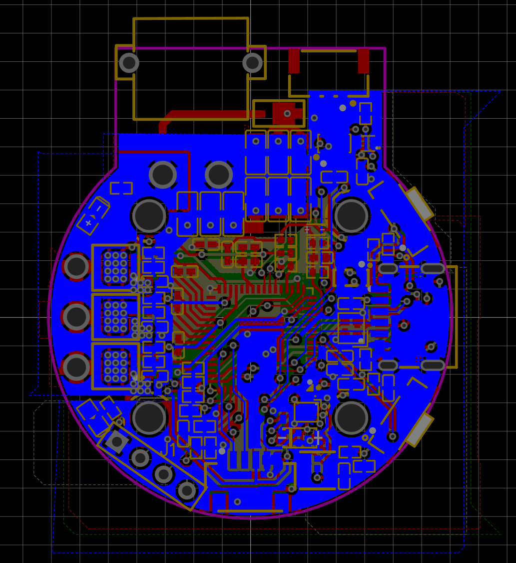
Re-did some of the schematic. I removed the resistors in-between the High and Low side mosfets. I saw some designs out there that don’t have these so I hope it’s okay. Also moved the mosfet capacitors to ground after the current sense resistors since it’s really close to power ground on the pcb. Also switched some of pins like the encoder, and used a different diode for the buck, the rest should be the same.
Tried my best to follow good practices for the board layout and design. I did a 4 layer stack up with Layers 1 and 2 being signal, ground, and power. With most of layer 2 being ground, Layer 3 is ground and layer 4 having VM power, motor-ground, and signals. The motor-ground and ground are connected through a 1mm trace on layer 4. I had to pass the VM power through vias from layer 4 to 1, which doesn’t seem ideal, but hoping will work. I used 7 VM vias for each at an estimated 12 amps capacity.
The opamp 1- and 2- run from the power ground plane under the current sense resistors ground as an isolated trace to the opamp- pin on the mcu.
Was also able to squeeze another 15uF capacitor onto the board for VM.
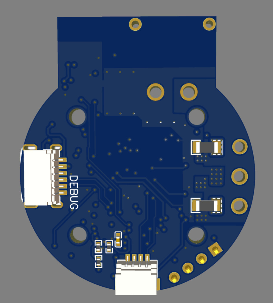
I wanted it to only be 1 sided but due to size constraints and also being a novice at pcb design. I had to put some passives and the sense resistors on the bottom side.