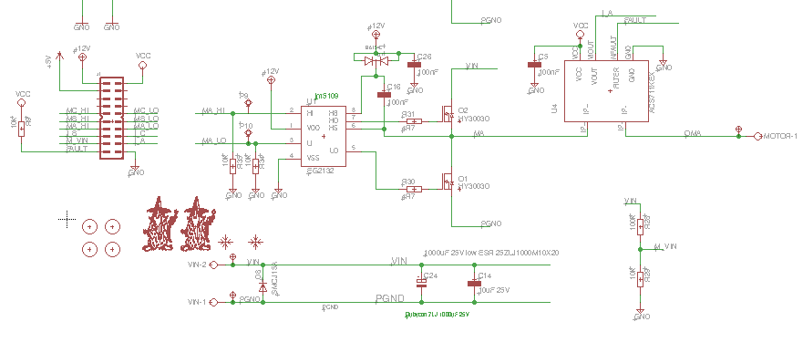
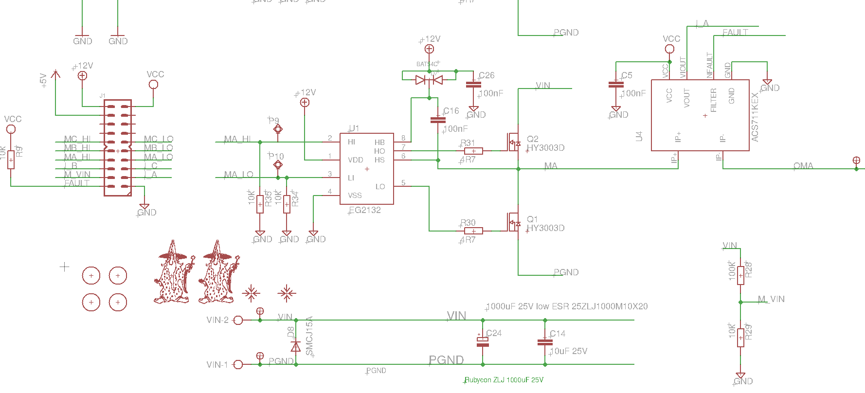
I didn’t include the other channels in this screenshot, but they are identical. Any suggestions? Any blatant errors?
I really would like to help
unfortunatly, picture def is too low
best regards
mmm yes
schematics seems to be a zoom .. I can see cutted lines ….
please leave complete schematics. errors hide in “non visible” parts
HI
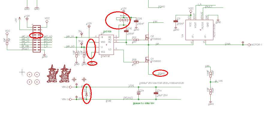
-add a resistance in charge pump, set it to 10R , to limit rush current that can , after time, kill diode
-use only ONE gnd, one big , solid ground plane,…. Pgnd and Gnd and Agnd are mess
-where are caps for H bridge driver
-add GND lines into your connector, and blend them across signals please.
-no sure a transil can handle voltage generated by free wheeling, please , what are your figures , consider an active clamp if necessary
Thanks!
-
I have 6000+ copies of the gate-driver, bat54 100nF circuit “in the field”. There have been other problems, but not the diode giving up. I will put a 4R7 in there as opposed to 10R to reduce manufacturing costs: The 4R7 is already present in the circuit, 10R is not.
-
I will connect PGND with system GND near the gate drivers. This should hopefully keep the gate charge and discharge spikes away from my “system ground”. In this board there are three gate drivers, so one will have to be the lucky one to get the system ground. Both PGND and GND are full ground planes, in that part of the circuit.
-
“where are caps” → You got me concerned…. Ooops did I forget. But I found them in the layout and then in the circuit as well: you can see C26 above. It is tactically placed as close as possible to the driver chip.
-
More ground lines in connector. Ok Good idea. Will do for next revision.
-
Free wheeling is not the problem. Braking is. The physical component looks as if it can handle about 2W. (Datasheet says 0.8kW or 1.5kW I don’t remember, I don’t care. But that’s “peak” and meant for transients. ) When braking a significant amount of mechanical energy can be converted back into electrical energy. For that, this board has no arrangements. If you need to be able to brake, you need to power this from a battery. (or a battery in parallel with a powersupply. 3S and 12V go together nicely. )
Thanks very much for your “second set of eyes”. Much appreciated. By now I’ve already had the PCBs manufactured and I’ve done a PNP run. I was intending to make 4 copies, but we screwed up and cleaned up the solder paste before doing the second panel. I do want to keep 2 for testing here, but I’ll make a second batch in a couple of weeks (if there are no show-stoppers in the first two). If you want a copy, send me a PM with your address.
I have 6000+ copies of the gate-driver, bat54 100nF circuit “in the field”. There have been other problems, but not the diode giving up. I will put a 4R7 in there as opposed to 10R to reduce manufacturing costs: The 4R7 is already present in the circuit, 10R is not
BAT54 really? IFsm is 600mA, at first low side activation , a large current spike circulate through 100nF and the diode.
please … add the resistance….
This should hopefully keep the gate charge and discharge spikes away from my “system ground”
it is a very common and large mistake from beginners to split “gnd” . GND is the “equipotential reference” , large plane, on several layers with vias between them is the best way to lower drastically high frequency impedance. I’m curious to see your layout.
“where are caps” → You got me concerned….
it is preferable to place critical component where there are used, also on the schematics. expecially when one ask for a pair review ![]()
More ground lines in connector. Ok Good idea. Will do for next revision.
it is also a common mistake from newbee, the rule is “alwas think about the return path”, critical for high speed , high rise up rate signal . twist cables, sputter gnd around signals.
I bet you also will use ribbon cables right??? remember => two wires close each others make a good air transformer 1:1 ratio :-/
Free wheeling is not the problem. Braking is. The physical component looks as if it can handle about 2W. (Datasheet says 0.8kW or 1.5kW I don’t remember, I don’t care. But that’s “peak” and meant for transients. )
OK a peak… right, so now, you must write down some figures … I warned you about the concern : this kind of component aren’t build for dissipating energy…
back on the :
I have 6000+ copies of the gate-driver, bat54 100nF circuit “in the field”
only a far less copies of my design… above your head in orbit… and nobody with a tall enough ladder to find and fix issues… ![]() , that’s probably why I’m a little bit peaky
, that’s probably why I’m a little bit peaky
If you want a copy, send me a PM with your address.
where are you located sir? (I’m in France) … probably far away from your lab…
I am in the Netherlands (Pays Bas) (lab). and in France (no lab ![]() ) next week. I have a reasonably good deal with DHL to ship stuff (across the globe!) for very reasonable prices. This is a reasonably cheap board for me to make, most of the components are the same as in the 6000+ sold project.
) next week. I have a reasonably good deal with DHL to ship stuff (across the globe!) for very reasonable prices. This is a reasonably cheap board for me to make, most of the components are the same as in the 6000+ sold project.
If you are between Toulon and Frejus I could drop it by next week.