Yes, you just need to use the resistor sense method. Then it will be fully compatible with SimpleFOC. Alternatively you can just live with lower current (10A). This way the MOSFETs will not heat up, and the current sense will still be accurate enough, and it will also be compatible with SimpleFOC given you use a lower switching frequency (25KHz) to relax timing requirements.
I should probably mention that if you use the DRV8323 you will have to write firmware which communicates with the driver to set all the settings, such as CSA gain, PWM mode, gate resistor value (gate drive current), etc. This is not provided with SimpleFOC so you will have to do this yourself.
Usage of smart gate driver like DRV83xx will help me avoid the gate resistor selection routine and provide with some protection. However the firmware will get a bit complicated for me.
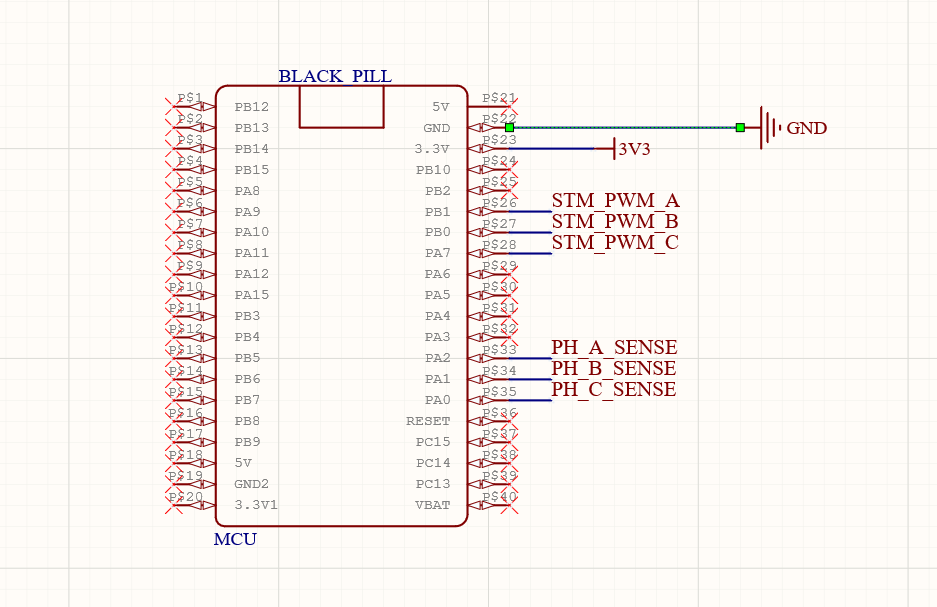
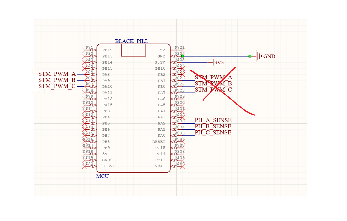
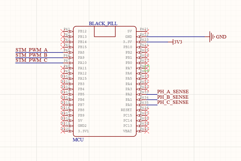
I can go ahead with corrections in my design itself with addition of MCU and current sense setup. Will that suffice or you suggest any more additions in my original design?
A smart gate driver will only provide protection if the settings are configured correctly, it is not as foolproof as an Integrated FET driver. It is up to you what other features you want in your design and it is not something I can decide.
My suggestions are to
fix the small traces
decide to fix your current gate driver circuit or switch to DRV8323 if you like it better
add current sense and MCU on the PCB
switch MOSFET to lower resistance one
use 4 or 6 layer PCB
If you want, you can make a copy of my design and start from there, it could save you some effort.
Do you want to continue with an integrated FET design or a discrete FET design? I am not sure why you would need lower resistance MOSFETs if you want to proceed with the integrated FET design. Or are you planning to start with integrated and move to discrete later?
The SimpleFOC PowerShield you linked is not a good place to start, it uses half bridges with integrated drivers but those are really old and they have extremely long switching times, meaning you won’t get good performance and it will heat up due to switching loss and you can’t run high PWM frequency which limits maximum motor speed. It is also not foolproof, because the overcurrent protection threshold seems to be set at 60 amps, which is way too high.
If you would like to start with an integrated FET design, you can check out my previous motor driver based off the DRV8316 https://easyeda.com/editor#id=|99132368fc384463a48528e5faa7b4ee|19356f95894c45c1ad31805f8862b7ef (copy and paste, clicking doesn’t work). I have already produced these boards and can guarantee it works with my custom firmware, but I haven’t validated SimpleFOC on them. It is an 8 layer design due to a special offer from JLCPCB but you can remove 3 internal GND planes and the internal VCC plane to make it 4 layers.
Just remember with an integrated FET design you won’t get much current, as the MOSFETs in the DRV8316 are 50 milliohms, I am able to get 8A (Peak, 5.6A RMS) for 1 second and 5A (Peak, 3.5A RMS) for at least 2 minutes before overheating.
My apologies, I meant Discrete FET design. For me the task currently is to understand working of SimpleFOC and start using BLDCs in my existing workflow.
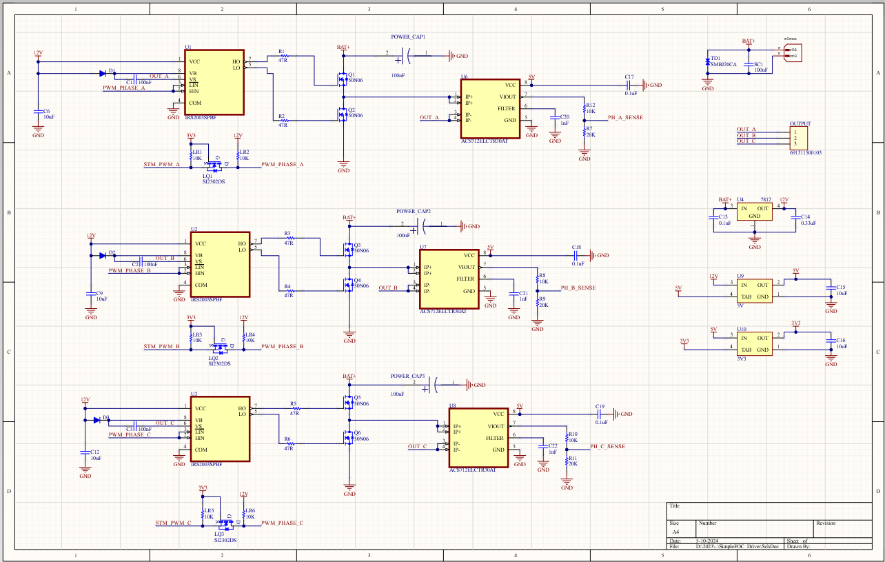
Noted that the Powershield current sensing seems to be handled by the BTN drivers as well, through the Is pin.
From a quick search the most readily available and easier for me to integrate is ACS712 based approach. https://community.simplefoc.com/t/asc712-current-sensors/1948/5
Above thread explains how to add it in my setup, Is there anything I should be aware of before implementing above explaination?
The ASC712 is an isolated hall effect current sensor with 80KHz bandwidth. It is probably the easiest way to get started with current sensing. Just be aware it is usually used as an inline current sensor which makes the software side easier, and if you are considering low side current sensing in the future (usually cheaper to implement) then you will need to plan for it now as there are some timing requirements to be aware of (which most likely are handled by SimpleFOC).
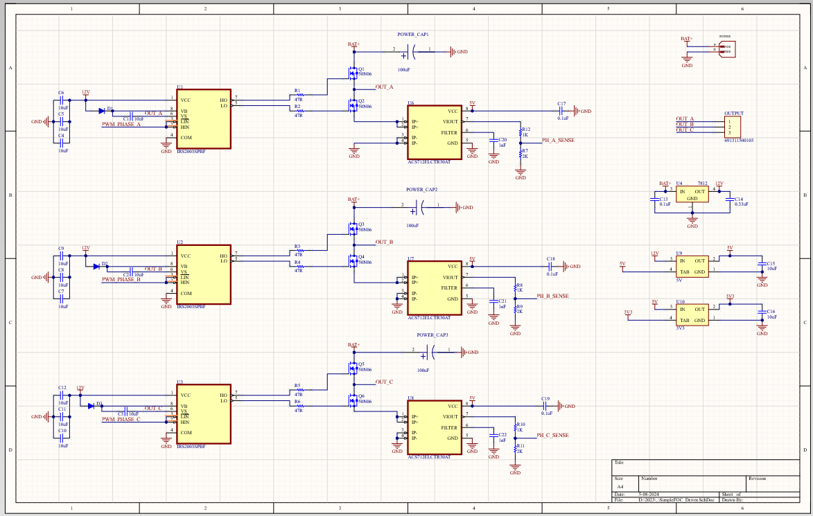
You are using an LDO ladder to drop to 3v. This is OK for an educational board to learn the basics but a poor design choice for anything else.
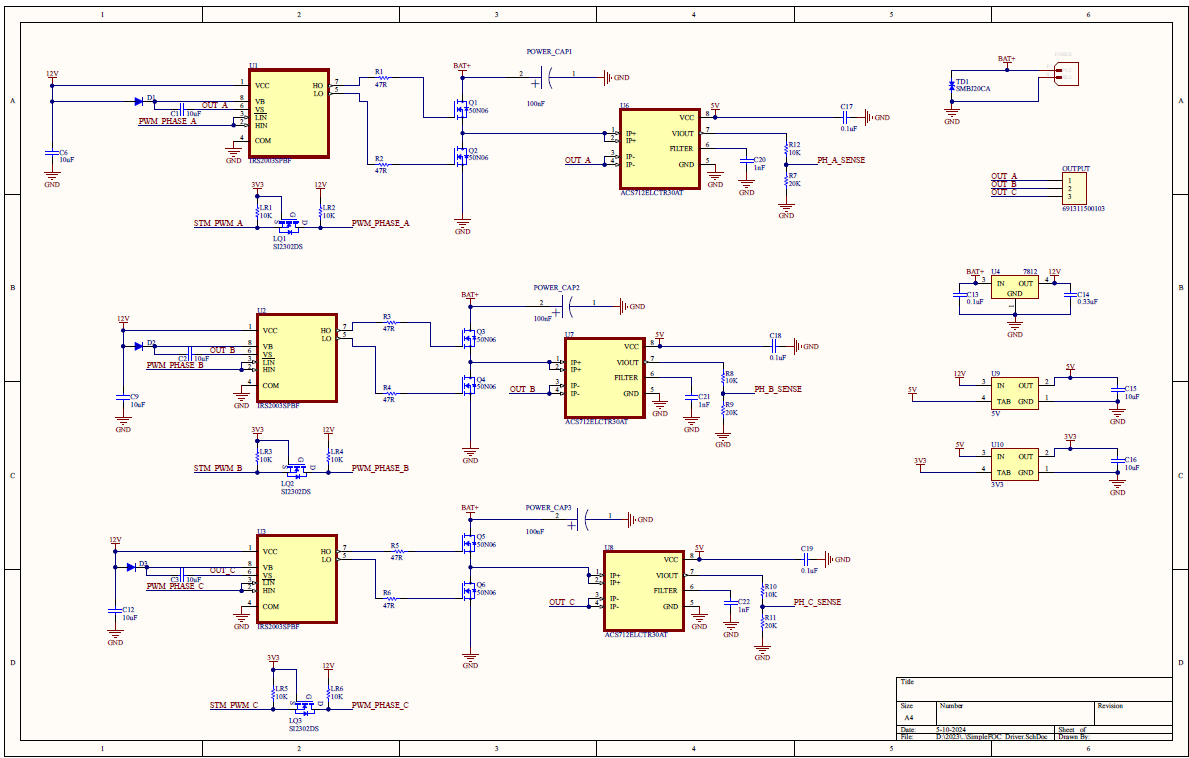
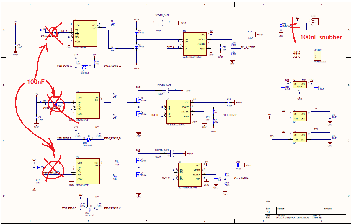
30uF bulk ceramics on each of the drivers is unnecessary. 10uF is enough.
There are no snubbers or TVS diode protection on the inputs? Living dangerously, I see.
Using such nice current sensors only on the low side sensing instead of inline is a waste of design potential.
10uF on the boost is way too high. At high PWM / low duty you may not have time to charge it leading to incomplete gate charge and mosfets operating in the high ohmmic region / overheating. Please check the mosfet total gate charge, and use the recommended ones. Especially because 2003 driver with an inverting input generates its own deadtime for the low side which means your signals are NOT center aligned but leading edge aligned and at low duty/high PWM the low side is even thinner. When your board smokes, Aladdin’s Djihnn wont come to fulfill a wish for a new one. I’ve tried.
You supply the driver with 12V VCC but drive the logic with what? 12V 5V? 3.3V? Please read the specs VERY carefully, as you are about to step into a world of hurt.
Thanks Valentine, you’ve given me quite a bit of homework.
I’ll clarify my way of achieving my goal with some context. I have always struggled to foolproof closed loop mode with SimpleFOC before because of lack of proper hardware. My goal hence is to achieve that with maximum scalability (I should be able to source components and recreate the boards on demand without importing ICs).
I’ll do this in iterations, first being a POC only. Just to learn the “what not to do”.
Enhancements will be done once I have successfully spun my 5010 both sides.
Now, Before cleaning my mess, I want to confirm if the solutions I am thinking of are right. Please help me with that.
Agreed, will switch to a much better power section in later versions.
Will switch to single 10uF on the driver inputs.
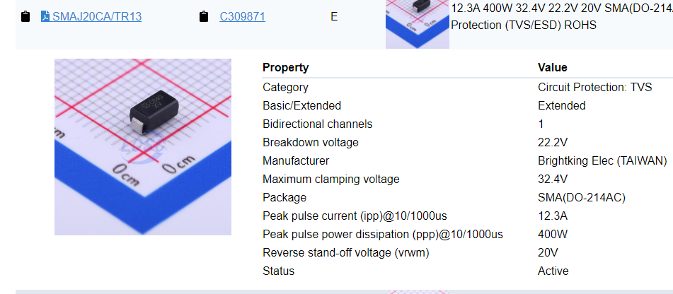
Will add the MCU Part and protection to inputs. Planning to add a SMBJ3V3CA TVS diode at each input
I saw in another post where the how-to for these sensors was to directly add them in the path of motor. Will implement it as is.
Understood, switched to a better? mosfet “CSD185101Q5B” . Lower Rds (1.2mOHM) , GateCharge Gate-to-Drain is 21 nC . That is about 1uF for 14V/18V. Will add this value as a boost cap.
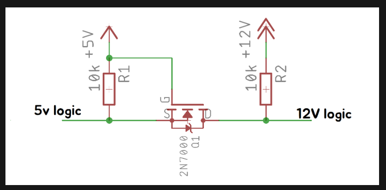
Logic will be driven by 3v3, do not want to mess with the STM32 logic levels. Noticed that the HI and LI pins are rated VCC, hence planning to add a transistor to bring up the 3v3 to 12V.
That’s 100nF boost cap equivalent. 1uF is too much. No need to change the mosfets. This is educational, not production grade board. If you don’t burn it, you havent learned.
You can use an external voltage translator/shifter, as long as you know what are you doing. Don’t overcomplicate your circuit. Just buy it.