Hello everyone. You may have seen my “RP2040 dual motor driver” board floating around the internet. I recently realized that making the power driver section modular and moving towards a dual sided board design had a lot of advantages, and so this week this driver board was born. So far my inverter layout on previous designs has mostly worked, but I had some long traces to run gate drive signals under some long power planes, and I think this led to issues where in some cases parasitic turn on of the opposite FET would result in catastrophic failure. I realized that with a dual sided design, my gate drivers lined up very nicely right with the FET gates, and the long runs could be completely eliminated. With improvements to the miller clamp circuit and improved snubbers, I hope this design will eliminate the catastrophic failures I was seeing.
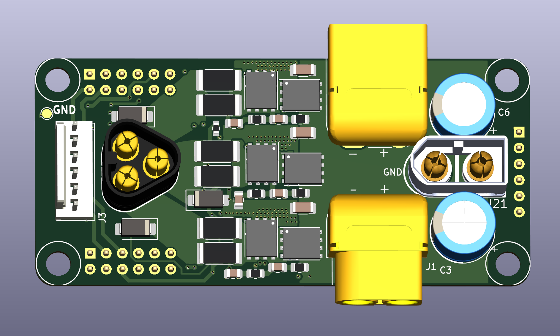

This design allows for daisy chaining power in medium power applications, or each board can be wired for its own power if needed.
Notably, there is no CPU on this module so you are no longer tied to the RP2040. I love working with the RP2040 and for my application, moving big slow drive motors for a farming robot, the 8khz loop rate I get is fine (also I see some redundancy in the code that could improve that somewhat). However some want better ADCs and floating point, and with this new board it will be easy to make other CPU drivers for it. Note that (I believe) I broke out the necessary pins for sensorless control, even though I will not use that, so this should be a more general purpose board for others to experiment with. Also the six pin connector next to the motor connector is for an encoder, and when used as I intend (tested already on my previous board design) would support hall sensors, SPI sensors, I2C feedback systems, and incremental encoders, plus thermistor feedback.
The board is on github now, under the “driver_module” kicad files here:
The board is 100% routed, but I have not fully gone over it for review. I would love your feedback on where it is so far.
One thing of note is that I laid out the interface connector with a pinout which is convenient for this specific board layout. I literally changed the pinout based on where traces ended up for the cleanest possible layout, but you can easily imagine a more universal pinout for something like this, with certain pins laid out in logical groups rather than individual pins placed wherever traces land. As you can imagine, if we as a community made lots of different boards with lots of different pinouts, it would be a headache for compatibility.
That said I am eager to produce these boards and get them tested as I have a need for functional boards as soon as possible so I am not going to fret much about that last point, but I am curious for any thoughts on community strategies for pinouts.
And all other feedback is appreciated!