Yes, the ceramic capacitors are “last resort” buffer in case you just want to do some really small testing without a large electrolytic capacitor, so that you got enough buffer to run the buck converter when the motor draws power. You must solder/attach a large bulk capacitor as close to the board as possible.
That’s a snubber.
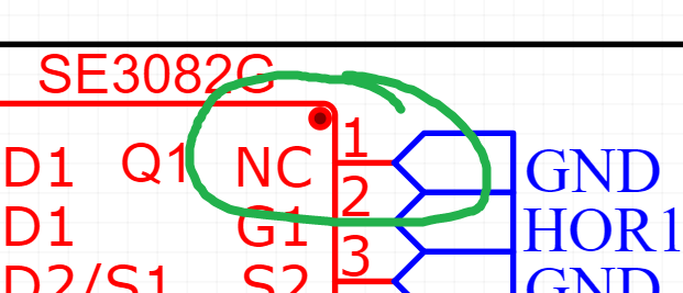
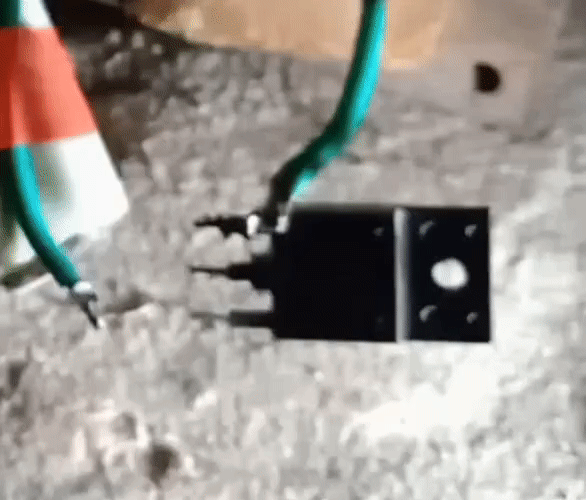
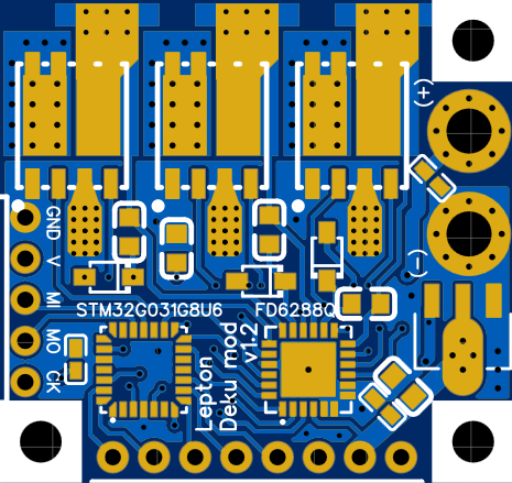
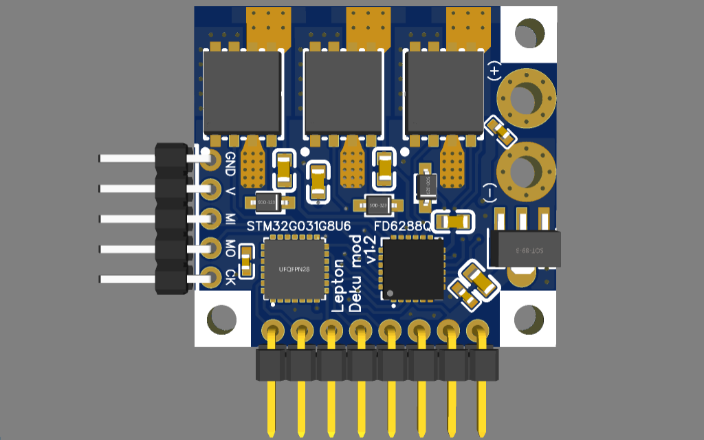
Pin 1 is NC so I assigned GND to keep things simple.
I have a 4-layer board where the vias on the pins serve a purpose (I routed the signal on the 2-nd layer). Yes you may delete them on the 2-layer board they don’t do anything.
Ah, that’s more useful than I thought. I figured it was just putting some free space to use.
Here’s another fun idea: after soldering thick conductors along the back side of the board, we could also hand solder a bunch of 1206 capacitors between them. It looks like you could fit 10 or 11. LCSC has up to 47uF with 25V rating which would be fine for me since I’ll be running on 3 or 4 cell lipo, so with around 500uF total I shouldn’t even need an electrolytic.
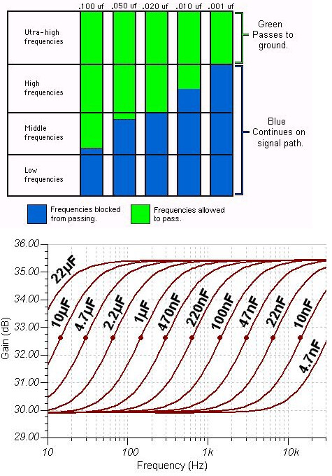
I read the article, but I still don’t understand what difference it makes when there’s so much other capacitance at about the same distance from the MOSFETs. Does the smaller size capacitor damp out different frequencies or something?
Oops, should have looked more closely at the datasheet Two pins for D1 and two for D2, I assumed there would be two for S as well.
In simple terms, snubbers form an R-L-C filter and protect the circuit from spikes. The large capacitance cannot match the small copper conductor inductance and resistance and they cannot absorb certain frequencies, they let them through.
I still don’t see why the small capacitor would function independently in this situation. lecture13.pdf shows that too, on page 25. Capacitors in parallel, Z = 1/(j*2piF(C1+C2))
And thinking more about that single S2 pin on the MOSFETs, won’t that significantly limit current at high speed? At low speed where you get high phase current for low battery current, it should be fine since everything is circulating through the motor coils and along the battery+ rail and big MOSFET pads. But once the battery starts having to put out some Amps, I’d think that little pin would get very hot very fast. The datasheet only gives numbers for drain current, but says nothing about source current.
How much inductance can there be from less than 1mm of copper between it and the first 1206? I’ll take your word for it that it is “enough”, but then I can’t imagine that parallel impedance formula ever being applicable to real components.
Well you have conductivity, cross section and length, so I suppose the short length is the trick. But with only 0.22mm² footprint to conduct the concentrated heat away, I still have a hard time imagining you could get anywhere near 80A without localized solder melting. Although it will also conduct heat into the rest of the chip and out the surface and the other pads, so that helps some, but that’s going through lower conductivity material. I wonder what the internal structure looks like.
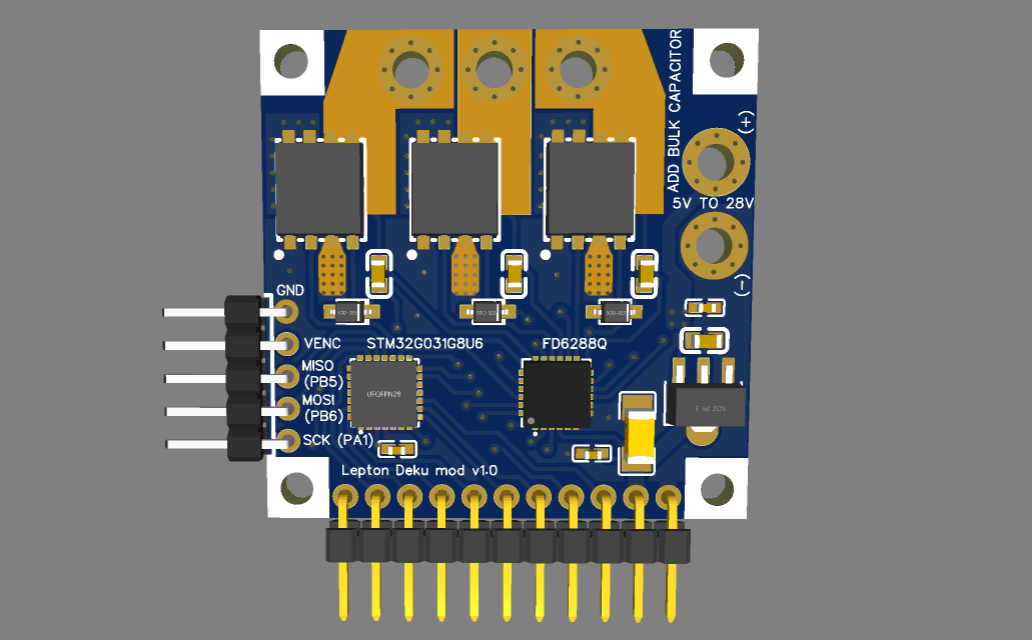
Unfortunately it looks like I’ll have to redesign for 6 separate MOSFETs anyway, because this type is almost out of stock and I don’t see any others like it with the internally connected S1-D2. Sadness. It was such a beautiful layout. Here was my final custom version. Maybe I will still order a batch of 5 with 1oz copper to test (heck, if short pinch points aren’t as bad as I was thinking then 2oz may not even be worth doing). If I’m lucky there will be more MOSFETs in stock by the time I need them.
The inductance comes from the input power wires and copper power plates. I believe we are reaching a point where I used to tell my students, “trust me, it works”.
P = (I^2) * (ρ * L / A)
where L is the length and A is the cross-area.
ρ ≈ 1.68 * 10^(-8) [Ω * m] —copper
I^2 = 100 [A^2] —10A current
L = 0.001 [m]
A = 10^(-6) [m^2]
P = 100 * 1.68 * 10^(-8) / 10^(-6) = 1.68 watts at 10A
I never claimed this board can pull 80A, actually if you read my initial post I explicitly said 10A is the max you could pull without 2oz/4layer plates before melting the solder.
Yeah I just wish I could understand why so I can apply the same thinking to other situations in the future.
You also said 40A with 2oz/4layer, and that’s not going to increase the cross section of the S2 pin or the contact area to conduct heat away from itself, so I was thinking we might still be limited to 10A battery current before melting despite being able to handle 40A phase current at low speed.
And if the MOSFET rating applies to the S2-D2 current and not just D1-D2 with the large pads, then 40A shouldn’t be anywhere near melting. I just have a hard time imagining how.
Put on a pair of goggles, hook up a motor, move away and give it a spin. If it doesn’t blow up, it’s good to go. If it does, well, you gained real-world experience and lost $20.
After deciding to stick with 1oz copper, I got curious if I could squeeze it down to 25x25mm when I don’t have to adhere to the 2oz clearance limits. In the end I arrived at 25x23.5mm, and I didn’t even have to go below 0.2mm clearance. A slightly more reasonable midpoint of the exercise was 25x27mm, but then I realized I could remove the holes and solder the motor wires directly to the MOSFET pins if I also remove the upper left mounting hole. Who needs 4 mounting holes anyway? And I’ve used cheap ESCs that had similar sized solder pads without holes and never felt concerned for the wires falling off, so I expect it will work fine. There’s a nice trick, using vias to help pin the copper foil to the board to keep it from peeling up.
I had to give up the SWD pins, and reset is only accessible as an unlabeled solder pad on the back, and I changed C7 from 22uF to 10uF so I could use 0603 size. The LDO datasheet says to use 10uF for its capacitors anyway, so I changed C11 as well, although I could change it back if there’s a good reason for it to be 22uF.
So now I know that I could. The question is whether I should. I’m really not too cramped for size anyway so I could just order the 30x30mm, but this one sure is tempting.
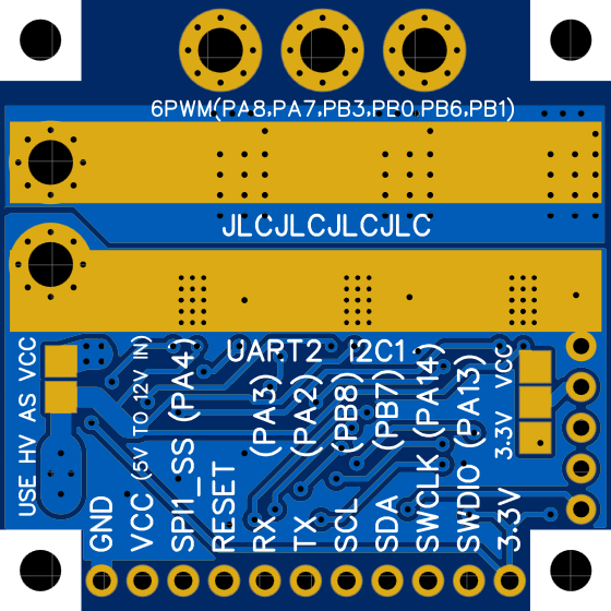
Is it possible to program this board without the SWD pins exposed? My research and testing with this board showed that both the I2C and the UART pins chosen are not compatible with the bootloader, meaning SWD would need to be used, unless you write a custom bootloader for the chip to support booting from those uart and i2c pins.
Thanks for the heads-up! I’m new to STM32, so I’m not familiar with the usual routine for compiling and uploading to it. I’ve got the Arduino IDE configured for the compiling part, and I was hoping to use it for uploading as well via an FTDI adapter to the UART pins like I’ve done with the Atmel-based Arduino Pro Mini, but if that’s not possible in its initial state then I’ll have to get the SWD pins exposed (and figure out what hardware and software I need to communicate with those…)
I think I’ll expand it out to my original target 25x25mm so I can relax the layout a bit and add a second 10uF capacitor so the LDO and gate driver don’t have to share the same one, and that should make room for a couple more solder pads on the back for the SWD pins.
No problem. Since you are re-routing most of the board anyway, it probably wouldn’t be hard to choose pins to break out that will work for the UART bootloader, and keeping your original compact layout.
Here is the reference to allowable programing interfaces.
Excellent job. The missing SWD will be an issue though.
Ha ha ha… true DIY statement. As long as someone’s life doesn’t depend on this or you are not using it on a one billion dollar rover mission to Mars you’ll be fine.
How are you going to program it then?
Good point here. I don’t see a way to program this.
Well, if anyone figures out a way to do this then let us know. Meanwhile, you can go for my Mosquito trick and use 1.25 mm headers instead of 2.54. You can fit twice as many pins. Also if you go for 4 layers you can improve heat dissipation and route more densely.
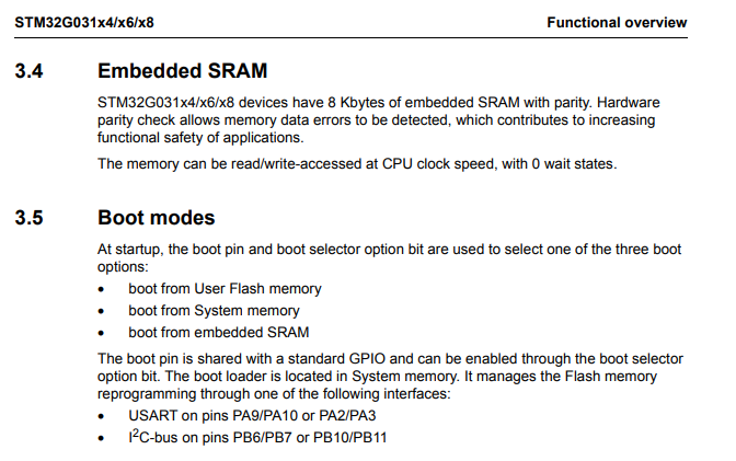
I just wish it said what combination of boot pin and selector does what As well as the initial state of the boot selector bit. USART on pins PA2/PA3 is what I want. I can’t use PB6 for I2C because it’s one of the TIM1 outputs, and this 28 pin package doesn’t even have PA9/PA10 or PB10/PB11.
Yeah, I’ll get those SWD pins accessible.
I was planning to solder wires to the holes rather than installing the pin headers that appear in the 3D model (hence the desire for large holes), but 1.25mm with pins is an option. That would also make room for CSS over on the encoder header, for any kinds that can’t simply be hardwired selected all the time. Though personally I’ll be using hall sensors (hopefully linear type, if the stator field doesn’t interfere too much at high power).
I’m having a hard enough time keeping track of routing on two layers, so I’d rather not deal with 4 just yet But hopefully someday I’ll have the skills (and the budget) for such work.
So, if you still have the boot0 [PA14] pin broken out, you can tell the stm32g031 to go into bootloader mode AKA look at PA2/PA3 or PA9/PA10 for uart input. Then, you can connect STM32Programmer over USART and it is basically equivalent to using the SWD pins.
The reason I am reiterating this is because you have the option to use PA2/PA3 or PA9/PA10, as they are available via alternate pin mapping (see picture). Additionally, the original board had I2C2 pins (PA9/PA10) labeled on the schematic, but not broken out to a connector. It seems this board is just itching to have full USART support!
(Also this is sort of a vicarious effort on my part, since I don’t know much about PCB design lol)
PA14 is the presently-unavailable SWCLK, so I’ll have to get it accessible. Maybe if I get CSS on the encoder header, its former pin can be repurposed for this, and I can have my easy FTDI interface. But then I’m only one pin short of proper SWD access…
Do you know if it will have to be manually reset after every upload of a new program, or if it will auto-execute like Atmel-based Arduinos? I stuck that reset solder pad on there just incase, but it would be nice to know for sure whether it’s needed.
So that’s what the PA9/PA10 in brackets meant Those are already accessible as MOSI and MISO, so maybe either that or PA2/PA3 will work regardless of the initial state of the boot selector bit.
So unless you want to have problems you should definitely provide a way to access the SWD pins. They will not only allow debugging, SWD will allow programming in any situation, while UART or other options depend on you getting into the boot loader…
You should also expose nRST for a seamless experience.
To use SWD you need a STLink programmer, the STLink Mini v3 is cheap and ideally suited, but if it’s not available, an STLink v2 (there are also clones) is enough…
To use it you need the following connections:
gnd
swclk
swdio
nRST
vdd (output to STLink, not input)