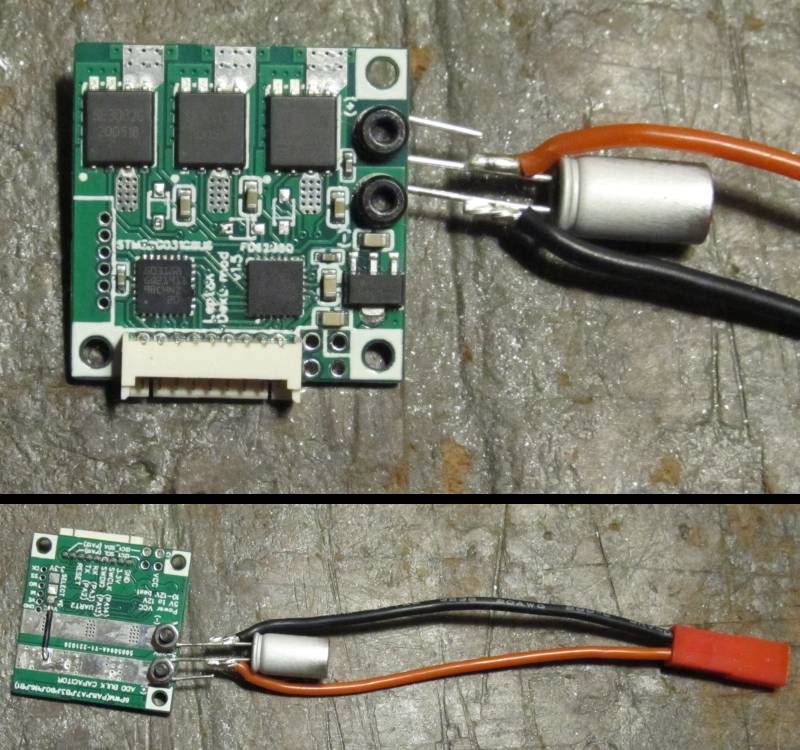
At long last I’ve acquired a bit of useful information! Lepton does work with DRV8300 after all. It was some combination of other damage and poor soldering skills that resulted in the failures on the one I tried before.
I want to avoid ordering components from LCSC until I know for sure which direction I’m going, but I also wanted to test an FD6288Q that hadn’t been exposed to my crude stovetop reflow method. So it was with a heavy heart that I decided to pluck one off of an unused Lepton. A side benefit was getting to test one of the DRV8300’s I desoldered from GooserCS with the heat gun on a Lepton that’s never burnt a mosfet or been exposed to stovetop soldering.
Sadly after installing the good FD6288Q on Gooser3, it died immediately with a tiny wisp of smoke from the vicinity of the PWM input pins. They now show low resistance to ground, similar to the bad pins on the other two FD6288Q’s I’ve tried on this board. Odd that all three have burnt near a corner of the chip, but it’s been a different corner every time.
The Lepton, on the other hand, works perfectly. Bootstraps are boosting the high side gate voltage (using the internal diodes, since I removed the ones from the board), and mosfet outputs are showing a proper waveform. I also made a less hazardous screw-on battery cable for testing. It has a proper polarized connector, and is much easier to screw on since I don’t have to get both the wire and capacitor lead pinched under the screw.
So I can reasonably conclude that there is a circuit design error in GooserCS and Gooser3. The only possible thing I can think of is that I’m running the high gate traces on the top layer underneath the bootstrap capacitors (between the capacitor solder pads), while Lepton, Qvadrans, and the DRV8300 datasheet’s layout example use vias to get around them. Gate lines shown in red, capacitors outlined in green.
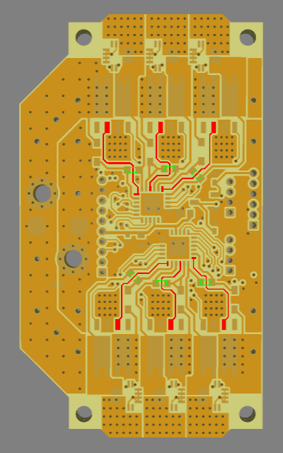
There shouldn’t be any significant inductive effects between a PCB trace and a capacitor, correct? The thickness of the soldermask over the gate trace could cause the capacitor to be very slightly off-kilter, resulting in a thicker solder layer between it and the board copper on one or both terminals, but I can’t imagine the tiny increase in resistance from that being such a consistent problem. And Lepton does have one low-side gate trace go between capacitor pads, though it is one of the 10uF power capacitors rather than a bootstrap.