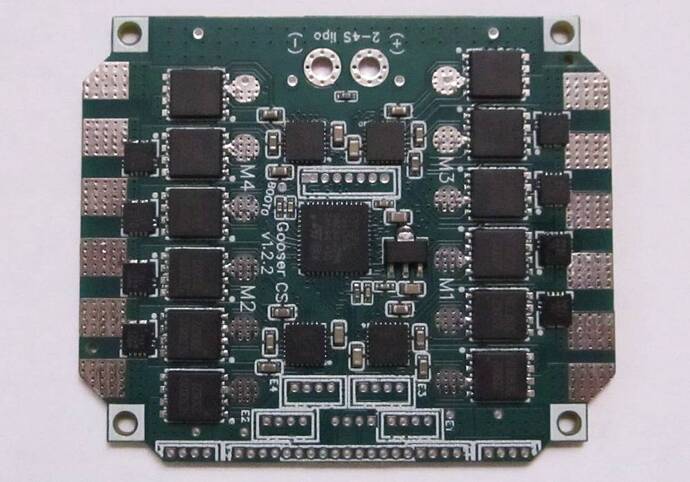
The boards have arrived! But the capacitors and connectors from LCSC may not be here for another week, so I can’t do any testing yet.
Nonetheless I have been preemptively writing the firmware. The most amusing problem I’ve discovered is that I should have called the motors M0-M3 instead of M1-M4, since the code is naturally zero-based. But I think it’s too much hassle to change at this point, since I’d want to rename all hall sensor and current sensor nets to match.
I found one minor hardware problem. I assumed there would only be one 100nF 0402 capacitor on the JLC basic parts list and used the first one I saw, but it turns it was only rated for 16V. Only the input snubber is exposed to high voltage, so that’s no problem to swap out on my boards while I’m soldering the ones on the back, and I’ve switched them all to the 50V version in EasyEDA.
The ADC configuration was fun. It’s much easier if you read the reference manual (rm0440 for this chip) to see how the hardware works rather than trying to understand it from the library interface. On Lepton I got so mad at the hideously cluttered LL and HAL libraries that I just wrote my own register #defines, but actually the official #defines for direct register access are reasonably well done so I’m using them this time. The DMA section of the manual is not entirely clear on how to set up for auto-triggering by ADC, so hopefully I did it right.
The general approach is to start the sampling for the next motor just before updating the current motor, so the next motor’s update will have recently-measured data ready to go without any waiting for the ADC. The ADC data is read by DMA into a circular array and then sorted out by using the pin numbers in the InlineCurrentSense and LinearHall classes as indices into that array.
/*
Current sense pins, phase A,B
M1 PB14 PB12 adc1 ch 5 11
M2 PF1 PA4   adc2 ch 10 17
M3 PB11 PB15 adc2 ch 14 15
M4 PA0 PF0   adc1 ch 1 10

Encoder pins
M1 PC4 PB2 adc2 ch 5 12
M2 PA2 PA3 adc1 ch 3 4
M3 PB1 PB0 adc1 ch 12 15
M4 PA6 PA7 adc2 ch 3 4
*/
LinearHall sensor[4] = {
  // Pin numbers are actually are indices into adcData[] (see ReadLinearHalls and ADC sequence config)
  LinearHall(3, 1, 6),
  LinearHall(4, 6, 7),
  LinearHall(10, 8, 7),
  LinearHall(13, 15, 7)
};
InlineCurrentSense currentSense[4] = {
  // Pin numbers are actually indices into adcData[] (see _readADCVoltageInline and ADC sequence config)
  InlineCurrentSense(15.0f/3.3f, 1.0f, 0, 2), // M1 and M2 have 15 amp sensors
  InlineCurrentSense(15.0f/3.3f, 1.0f, 5, 7),
  InlineCurrentSense(31.0f/3.3f, 1.0f, 9, 11), // M3 and M4 have 31 amp sensors
  InlineCurrentSense(31.0f/3.3f, 1.0f, 12, 14)
};

volatile uint16_t adcData[16];

void ReadLinearHalls(int hallA, int hallB, int *a, int *b) {
  *a = adcData[hallA];
  *b = adcData[hallB];
}

float _readADCVoltageInline(const int pin, const void*) {
  return adcData[pin] * (3.3f/16384.0f);
}

void setup() {
  RCC->AHB1ENR |= RCC_AHB1ENR_DMAMUX1EN | RCC_AHB1ENR_DMA1EN;
  RCC->AHB2ENR |= RCC_AHB2ENR_ADC12EN;
  RCC->CCIPR |= RCC_CCIPR_ADC12SEL_0; // ADC use PLL clock
  ADC1->CR = ADC2->CR = ADC_CR_ADVREGEN; // Enable voltage regulator
  delayMicroseconds(20); // Voltage regulator startup time from STM32G431 datasheet

  // Configure ADC to read one motor's halls and current sense per trigger event
  ADC12_COMMON->CCR = 6 | ADC_CCR_MDMA_1 | ADC_CCR_DMACFG; // Dual mode regular simultaneous, enable DMA (2 bytes per sample, circular)
  ADC1->CR = ADC2->CR = ADC_CR_ADEN | ADC_CR_ADVREGEN;
  ADC1->CFGR = ADC_CFGR_DISCEN | (ADC_CFGR_DISCNUM_0); // Each ADC reads two values per trigger
  ADC1->CFGR2 = ADC_CFGR2_ROVSE | ADC_CFGR2_OVSR_1; // 4x oversample, giving 0-16384 range
  #define ADCSQ(idx, ch) ((ch) << ((idx)*6)) // More concise than the ADC_SQRx_SQy #defines
  // Note: SQR1 low bits specify the number of conversions
  // Note: ADC1 and ADC2 can't convert the same channel number at the same time
  ADC1->SQR1 = 8 | ADCSQ(1,5) | ADCSQ(2,11) | ADCSQ(3,1) | ADCSQ(4,10); // M1,M4 current
  ADC1->SQR2 = ADCSQ(0,3) | ADCSQ(1,4) | ADCSQ(2,15) | ADCSQ(3,12); // M2,M3 hall
  ADC2->SQR1 = 8 | ADCSQ(1,11) | ADCSQ(2,5) | ADCSQ(3,3) | ADCSQ(4,4); // M1,M4 hall
  ADC2->SQR2 = ADCSQ(0,10) | ADCSQ(1,17) | ADCSQ(2,14) | ADCSQ(3,15); // M2,M3 current
  DMA1_Channel1->CCR = DMA_CCR_CIRC | DMA_CCR_MINC | DMA_CCR_PSIZE_1 | DMA_CCR_MSIZE_1;
  DMA1_Channel1->CNDTR = sizeof(adcData)/4;
  DMA1_Channel1->CPAR = (uint32_t)&ADC12_COMMON->CDR;
  DMA1_Channel1->CMAR = (uint32_t)&adcData;
  DMAMUX1->CCR = 5; // ADC1 (reference manual RM0440, page 420, table 91)
  ADC1->CR = ADC_CR_ADSTART;
...
}

void loop() {
  for (int i = 0; i < 4; i++) {
    while(!(ADC1->ISR & ADC2->ISR & ADC_ISR_ADRDY)){} // Make sure this motor's hall and current sense values are ready
    ADC1->CR = ADC_CR_ADSTART; // Start ADC for next motor
    motor[i].loopFOC();
    motor[i].move();
  }
}
Although I’ll need to use a different configuration during calibration since I won’t be able to keep requesting conversions during that. I think just setting ADC1->CFGR = ADC_CFGR_CONT will do it. That should loop through the whole sequence as quickly as possible until told to stop.
