Hello SimpleFOC Community,
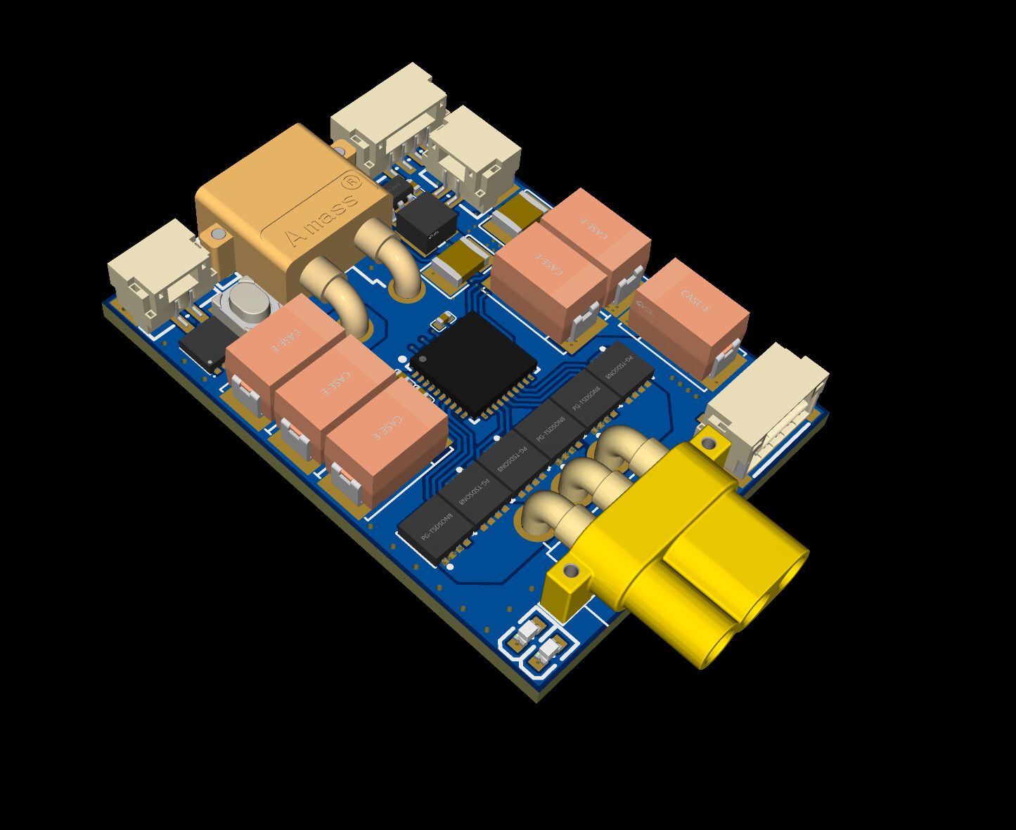
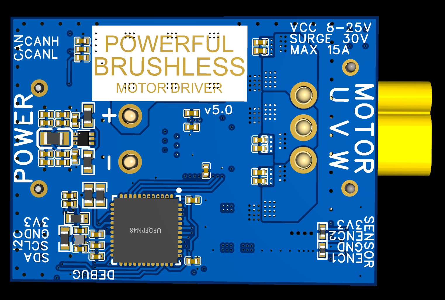
I’m working on a new motor driver with the main goals of medium current capability without needing cooling, and small board size of 30x50mm. I also want to experiment with reducing power losses in the current sensing by using the MOSFET RDS(on) to measure the current, inspired by the DRV8316.
I’ve included a XT30 connector for power and MR30 for the motor, and everything else uses JST GH connectors for maximum user friendliness. The board includes 600uF of capacitance so no external ones are needed, and the total height of everything is 7mm. The input voltage range is 12-25V, and the maximum continuous output current is 15A.
I’d like someone to have a look over my schematic and calculations to make sure I haven’t made any silly mistakes, and any feedback would be appreciated.
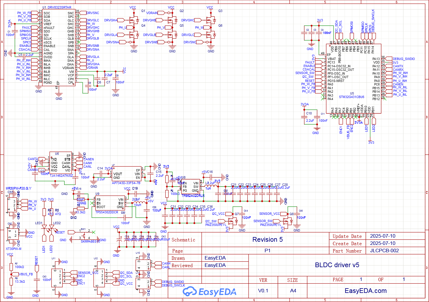
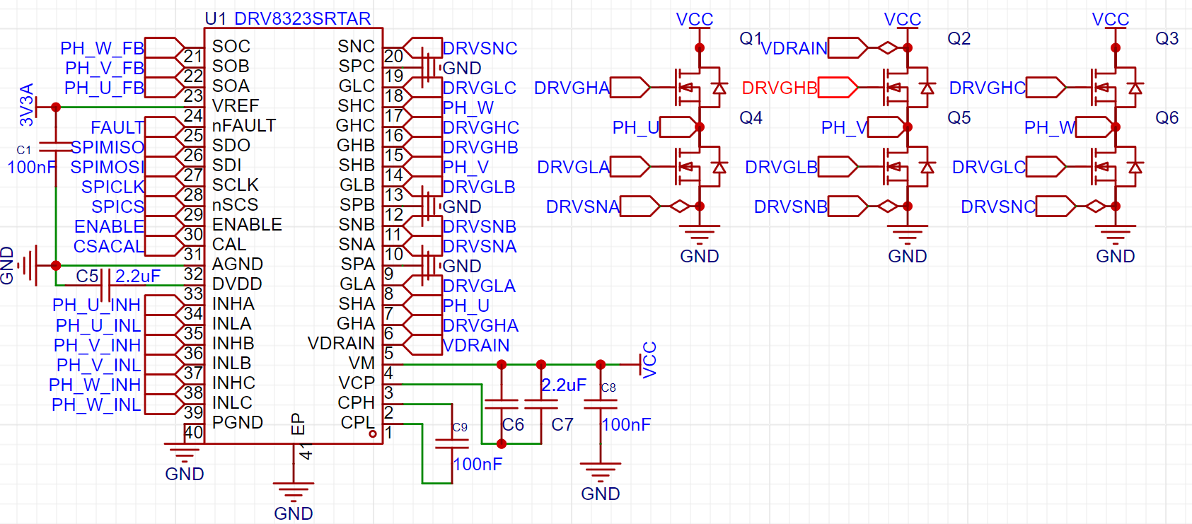
Driver:
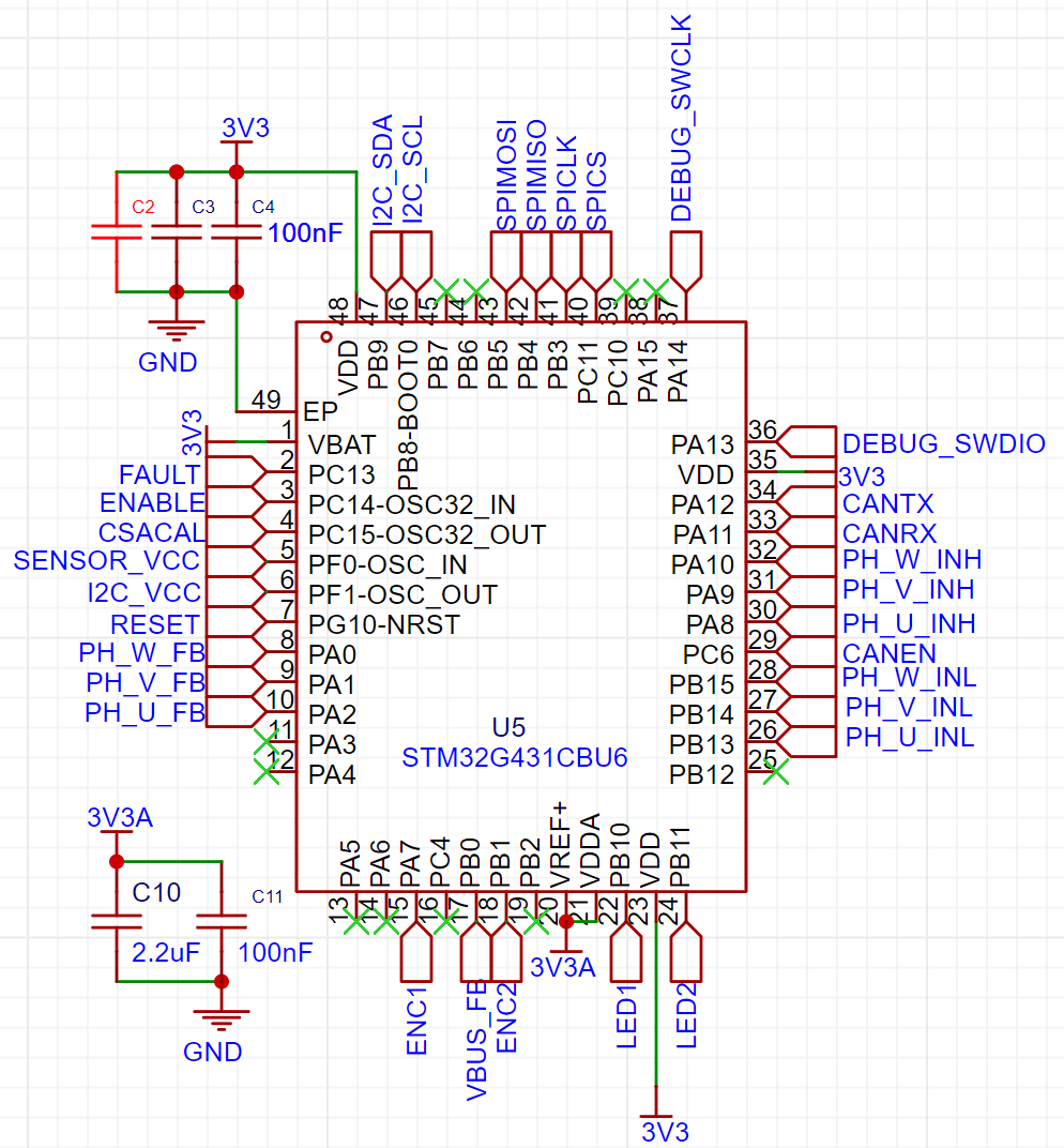
MCU:
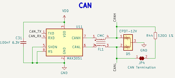
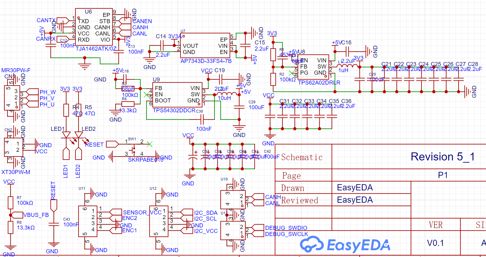
Power & Communication (It’s a bit messy I know):
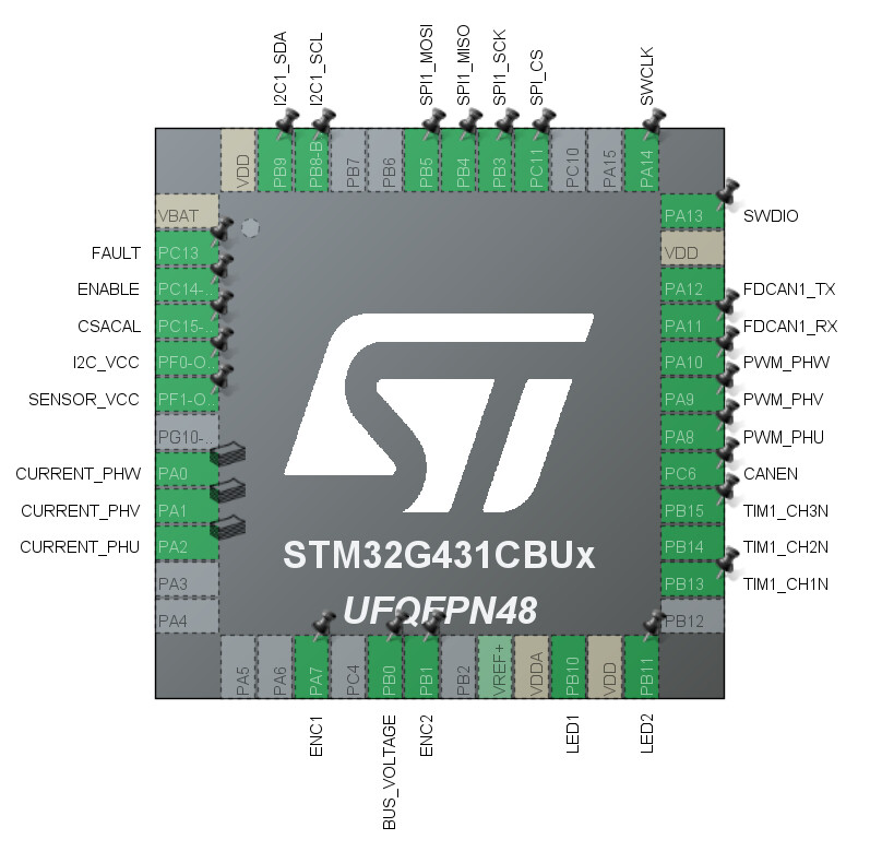
STM32CubeMX Pin Assignments:
The VCP and CPH-CPL capacitor values in the schematic are higher than values suggested by the datasheet, this is because of capacitor derating. The 2.2uF is a GRM155R61E225KE11D and 100nF is a GRM155R71H104KE14D. When you apply the derating due to DC bias at operating voltage (which you can find on the manufacturer website), the effective capacitances reduce to around 1uF and 47nF which is the recommended value in the datasheet.
The sensor I am using is a sin/cos encoder which is connected to the ADC, but I also want compatibility with incremental encoders, so the sensor pins also have comparators attached where the output will be internally redirected to TIM3 in encoder mode.
The MOSFET I am using is the BSZ0901NS. The RDS(on) varies between 1.7 milliohms at 25C and 2.7 milliohms at 150C. To compensate for this I will use the internal temperature sensor of the STM32 and a look up table to look up the effective gain of the amplifier based on the temperature. The PCB is 6 layers with 2oz copper on all layers, to improve heat transfer between the MOSFETs and the STM32 to ensure good accuracy of the temperature readings.
I will be running 50KHz PWM with Space Vector Modulation, pulled to GND to reduce switching losses. The current will be measured using 2 phases chosen on the fly (based on longest low side FET on time). Using center aligned PWM, I calculated the minimum on time of the low side FET to be 1.34us in the worst case where the MOSFET turns on immediately in the next switching cycle. The datasheet mentions that the current sense amplifier turns on after the 500ns Tdrive time when using RDS(on) sensing.
So the time is takes for the current sense output to become valid after the falling edge of the PWM is: 150ns (propagation delay) + 100ns (fall time of HS FET) + 50ns (dead time) + 500ns (Tdrive, including rise time of LS FET) + 600ns (CSA settling) = 1400ns. This means the current must be sampled 60ns after the start of the next PWM cycle. Since the propagation delay is 150ns, the low side FET will not turn off before then, and so the current will still be valid. This means the margin of error is only 90ns.
I will be using custom firmware for these advanced features so it is not a problem if they are not supported by SimpleFOC yet. But I still want to maintain compatibility with SimpleFOC where possible.
I’ve almost finished designing the PCB, so hopefully I haven’t make any mistakes or oversights that require a significant redesign.
Thanks,
Andrew