There was nothing wrong with the board.
- Schematics
The problem was that EasyEDA and Altium have incompatible component databases. When you import the Altium project into EasyEDA, the import assigns nothing for the components, I mean the link is broken, which means EasyEDA doesn’t know how to generate BOM and PnP, as well as cannot link the schematics to the PCB layout. This in turn breaks the workflow, which means when you make a change in the schematics you cannot update the PCB layout. Also you cannot order SMD with the board.
- PCB layout
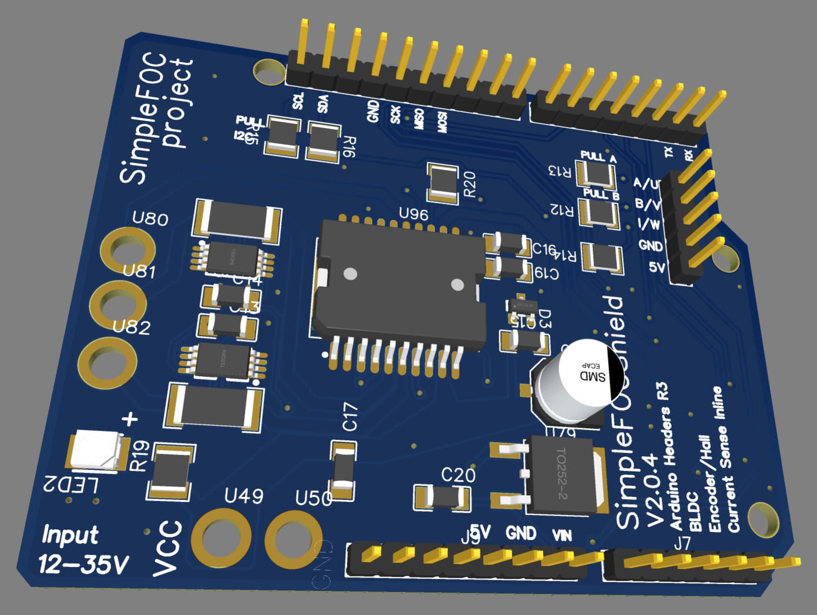
EasyEDA has very tight integration with the JLC’s manufacturing process. Which means the footprints are different from Altium’s “generic” footprints. Usually the EasyEDA footprints are larger than Altium’s, which means they cross over traces, and also Altium’s footprints don’t have enough area to “wet” the components and the components may form cold joints. Especially in your case this becomes a problem when you push very high current. Hence, the DRC fails, where they check the minimum distance between conducting copper surfaces.
- General PCB comments
The workflow is from schematics to PCB to manufacturing, obviously I am not saying anything new. However, with the component database link missing, everything falls apart. I tried keeping your schematics and replacing only the components. However, this failed due to footprint difference, because when I update the component I need to update the PCB, and the DRC failed. Also, it took a lot longer than simply creating a component list with the footprints, and re-creating the schematics from scratch rather than updating Altium’s import. It was a practical trade-off. The schematic was simple enough to be recreated in under one hour.
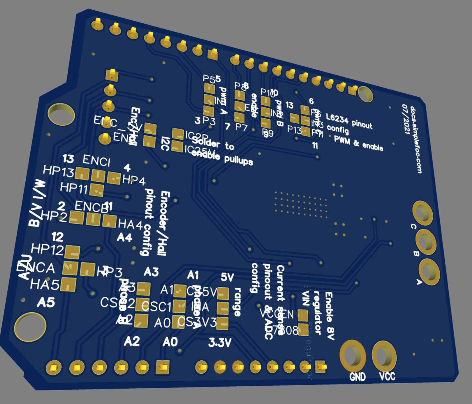
The PCB had to be redone again due to the footprint difference, as well as I saw some minor issues with the power tracks, where I built top/bottom areas with vias to allow for high current and better heat dissipation through the leads. Also, I widened the power tracks to 70mil (originally they were 30 mil IIRC). Below is original and re-worked.
Also please pay attention to the difference in Altium and EasyEDA footprint difference. EasyEDA’s is round, and longer, which steps over the adjacent tracks, in that case, the track net NETC3_1.
Once I replaced the components, I had to re-lay the PCB because EasyEDA wipes out the original layout. I am not sure if this is EasyEDA’s shortcoming or not, I didn’t write the backend so no idea but the result was a complete redo.
Lastly, the copper pour areas are re-layed because EasyEDA re-pours the copper areas with its own rules, which sometimes breaks the original design. Also, I added extra ground vias for better top/bottom connection and heat dissipation.
- OpAmp capacitors: I understand, I left one capacitor in the PCB, I manually replaced it, which means the PCB in the shared project doesn’t match my schematics. This can be fixed later.
Absolutely, this is for educational purposes. It’s a lot of fun and hopefully will inspire more people to get engaged. If the project is public, and EasyEDA is free and integrated with JLC, this would make it a lot more attractive to people who are willing to experiment.
Cheers,
Valentine