For now you will need the dev branch of SimpleFOC if you want to try it out, but it will be part of the next release.
I’m using the RP2350W, so far only in 6-step mode, which worked fine. Now I want to move to FOC. I designed a board rated 600 VDC with full isolation between Pico 2 and HV side. It has zero-crossing comparators, isolated current and bus-voltage sensing, plus braking. You’re welcome to copy it: https://carnetic.com/wp-content/uploads/2025/09/BLDC-Direct-by-RPI-Pico-fully-isolated.zip And if you know how to implement SimpleFOC, pls. reply.
The RP2350 is very fast, and the PWM generation works well.
But unfortunately it has basically the same poor ADC as the RP2040, no real improvements there for low side current sensing.
The problem is that the ADC is quite slow, and that we can’t trigger it well from the timers as we need for low side current sensing.
Even assuming you come up with a scheme to trigger the conversion, converting three phases will take a long time, and this will limit your performance in terms of the PWM frequencies you can use and the maximum voltage you can use proportionally to your power supply voltage.
So unfortunately the RP2350 is not recommended if current sensing is required…
Thanks Runger!, I suppose I will have to switch to STM32 at the end. [insert sad noise]
I have to say that using a Pi Pico is very tempting, especially for fast communications (Command update, sensor reading, introspection at the PWM frequency etc.)
I’m working on whole body robotics where many actuator needs to talk to each other or to a central computer with minimum latency and high frequency. This was the main reason for developing a TI based motor controller years ago.
Now that I’ve started playing with The RP2xxx MCU, I see the potential for that. With the help of existing project, and the great doc on PIOs I was able to implement RMII 100Mbps raw Ethernet without CPU overhead, or highs speed (12 to 30Mbps) RS485 bus with automatic instant reply (like profibus). The PIO can also be used to interface with virtually any industrial encoder or other sensors. It can also control many PWM channel for multi axis setup with high resolution and dead time management.
It’s true that the ADC is the main limitation.
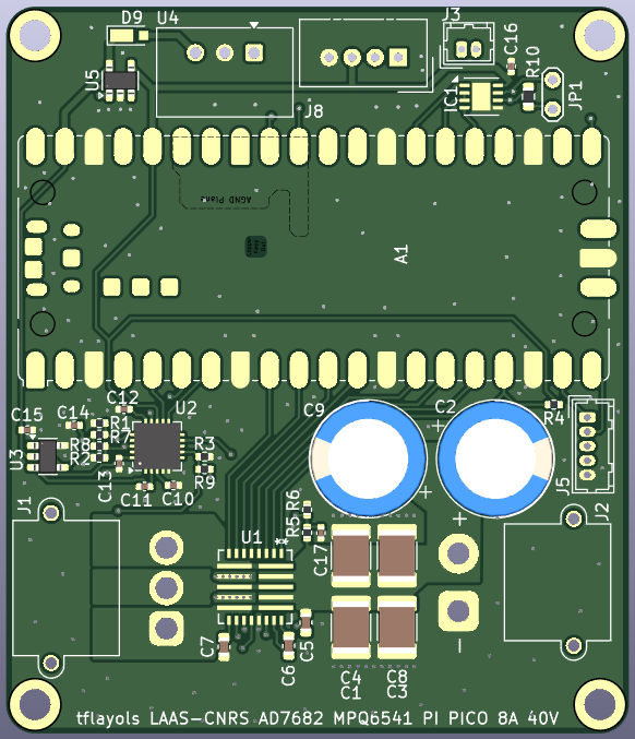
I’m considering making a custom dev board with an external SPI ADC. I’ve started a design here:
Perhaps, but PlatformIO is better for development, and the earlephilhower core has better performance than Arduino’s original one, so all in all I think this is a better way of working with the Pico 2 anyway…
Perhaps they will integrate it into the Arduino core eventually, but I would not hold my breath, TBH.
I’m currently stubborn my way designing with RP2350 and TI DRV8353 with low side current sensing. I know that RP2040 have no support on low side sensing,.do you think simpleFOC able to get the RP2350 work on low side sensing?
One last question @runger, is this still true for in-line current sensing for the RP2350? Saw in the doc that it can support in-line current sensing for pico.
After seeing how complex STM32 can be, I think I want to stick to RP2350.
With the latest release of SimpleFOC the RP2350 is now in the released library also…
I think supporting current sensing in an improved way would be a great addition for the RP2350, that’s an effort I would like to support!
I see from your schematics that it’s a low side sensing scheme with the MP6541, so I think some care has to be taken when designing the solution.
SPI attached ADCs seem like a good option, but looking at the AD7689 I don’t think it will be ideal. Here the nCS (CNV) signal would trigger the conversion, and you’d have to do two 48 bit reads to get the latest conversion result. And it’s only 250kS/s, so I think this will be slower than the RP2350 native ADC.
I think you would need the right kind of ADC chip that
A) supports an external trigger and
B) can then either sample 3 channels in parallel, or autonomously sample and convert 3 channels successively, and allow you to read out the results after the conversion.
Then you could trigger it at the right time (this I see as being feasible using the timers) for low side sensing, and read the results back afterwards, preferably also timer-triggered and using DMA…
The ADC you‘re looking for would have to support at least 1MS/s, ideally a bit more, and be able to convert 3 channels without extra delays in-between. You could also use 3x single channel chips, might be simpler to find suitable ones but would complicate the readout via SPI.
AD7091R looks like it might be feasible. Maybe. It will require some in-depth analysis of the Datasheet…
Thanks for your feedback,
I think you are right. The ADC is probably too slow.
When I first read the MP6541 datasheet, It was not clear to me what the analog output really was, since on the graphs, it seems that the current sensing is not modulated by the PWM, so that it would behave more like inline sensing.
Current-Sense Amplifiers
The internal current-sensing circuits detect the
current flowing in each of the three outputs. An
output pin for each phase sources or sinks a
current that is proportional to the current flowing
in each phase. It should be noted that only the
current flowing in the LS-FET is sensed in both
the forward and reverse directions
This is really not clear.
I think I will move away from both this ADC and the MP6541. It is hard to find a suitable ADC and going one 12 bits SAR per channel is a better idea. I wanted to evaluate the MP6541 to have a very compact design, but that is another sorry, I should keep the two project separated.
To keep the design compact still, since the PIO let us do deterministic data transfer, we could even choose a simpler SAR ADC where the conversion rate and logic is linked to the data transfer.
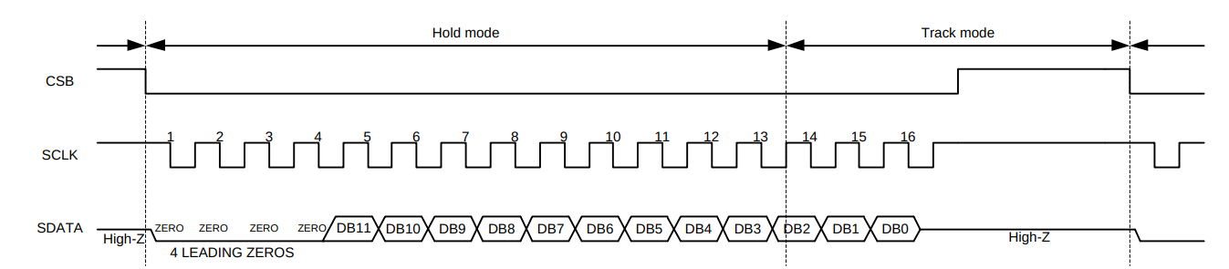
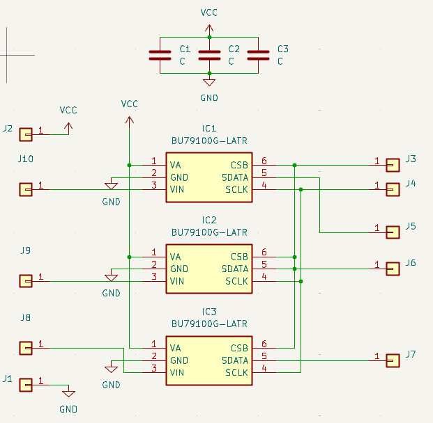
For example, with the BU79100G-LA (6pins 2.9 mm x 2.8 mm x 1.25 mm):
The maximum SPI frequency is 20Mhz, it needs 16 clock cycles to do the conversion and transfer, so a latency of 0.8 uS.
Thanks to the PIO again, we can use only 5 GPIO to do 3 current sensing (share CLK and CS + one data input per channel).
What do you think?
I have some BOOSTXL-DRV8323RX that I could use as power stage, and focus on the pico2 + ADC part.
I can’t really comment on the other points related to MP6541 or the relationship of the projects, except to say it’s quite a nice chip…
For the ADCs via PIO I think this is a really cool idea but would have to include error detection if there were the possibility for the 3 ADCs to somehow „desync“. But maybe this can be excluded already on the electrical protocol level.
I’m not very deep into the PIO programming (yet?) so I’m not sure what the best approach is. Triggering the ADC sample with the SPI sound tempting, but I think in practice it then means you have to do 2x 16 bit reads to get the desired result. So that is maybe something that doesn’t matter in practice, but certainly on paper it adds a bit of latency. A setup where you can trigger the conversion with another signal, and then read it after a short delay with 1 x 16 bit transfer may result in lower latency.
No, actually, the SPI would trigger the conversion just by initiating the data transfer, so it is exactly like if we had a dedicated signal. (we are not triggering the conversion by writing an SPI register)
The SAR conversion is happening at the rate of the SPI clock event.
The ADC conversion can be thought of in 3 distinct steps:
sample 2. conversion 3. output/transfer
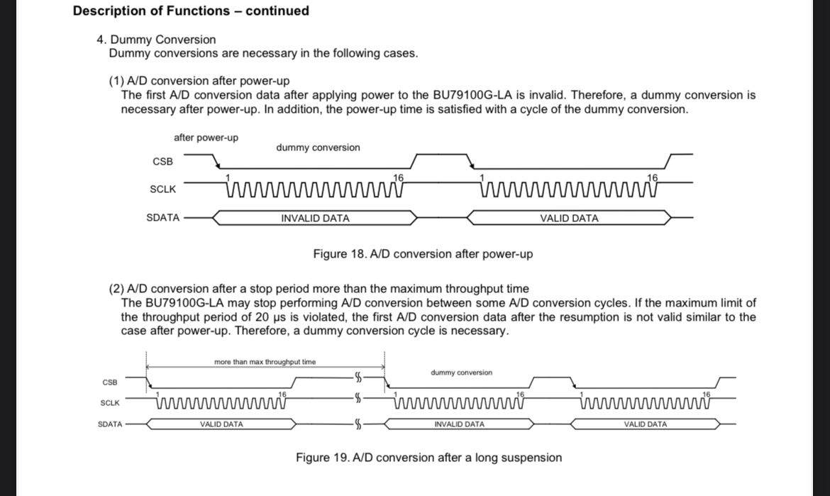
For the BU79100G it achieves high throughput and is triggered by the SPI nCS, but its performance depends on you reading it continuously.
The „sample“ stage is achieved by it continuously sampling the input („Track mode“ in its Datasheets terms) and then initiating the „conversion“ stage when nCS transitions low. It then performs the conversion and delivers the result within the 16 clocks you mentioned.
So far so good, but the problem is that you have to read near continuously, otherwise:
So looking at case 2, basically if the PWM frequency is less than 50kHz you would not meet this requirement and and would need 2x 16 bit reads. And 50kHz is quite fast, usually PWM speeds are more like 20-32kHz…
So I don’t think it’s a show-stopper but I do think a model with seperate trigger might be more suited to the low side sensing use case.
I don’t think it is problematic, the PIO would have no issues reading more often while still being in sync with the PWM, and only transferring the right samples via DMA.
I could make a proof of concept if it’s interesting for you.
I now have a proof of concept to read an external ADC with the PIO.
It uses one spare PWM for sync and one GPIO (that do not need to be connected to any external component, but can also be used to trigger ADC with independent trigger input.
This spare PWM is set to a fix duty cycle (calculated to compensate for dummy read, and or/sampling time centering).
In the case of the BU79100G, The PIO is waiting for this channel to go low, then read a dummy conversion, and then start the real one, it read the 3 ADC in parallel, and transfer the result via DMA.
Here are the few limitations:
The ADC data GPIO needs to be consecutive pins (limitation of PIO, but could be lifted by using 3 PIO State machine instead of one.)
The ADC samples are transmitted to the CPU with Interleaved bits (a0_bit0 a1_bit0 a2_bit0 a0_bit1 etc..) So the CPU as to deinterleave it in software. (I think this is marginal compared to FOC, but it could also be lifted using one PIO per ADC). Also, with RP2350 I think we can use UBFX/BFI instructions to do this efficiently.
This uses a GPIO only used for internal sync.
I still have to clean the code and finish the DMA or interrupt part to get the ADC value.
I’ll order some ADC to test it fully.
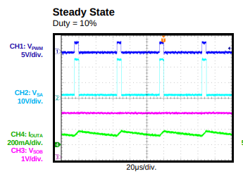
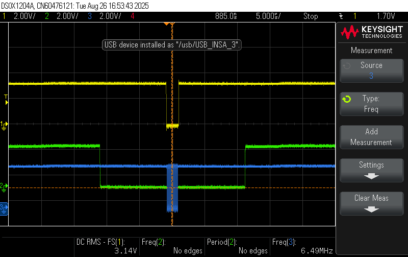
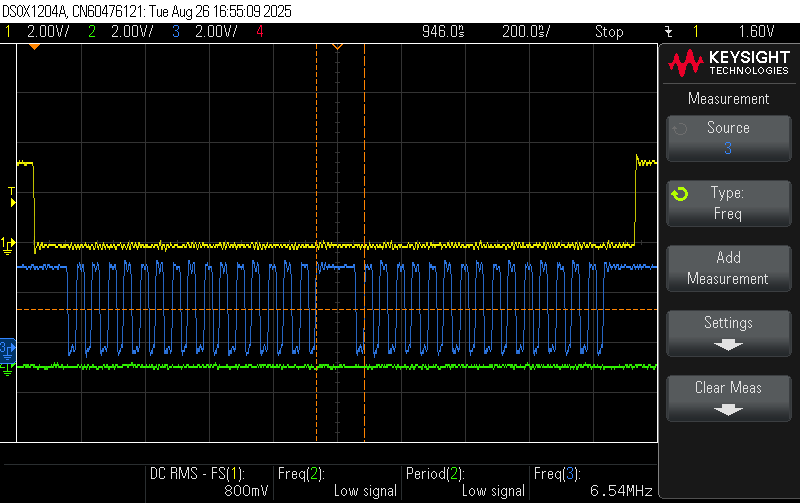
Here are some graphs:
In yellow, the additional fixed duty PWM, In Green one of the driver PWM, in Blue, the generated clock line.
I’ve made a branch in the drivers repository for the RP2350 current sensing:
You could make a PR based on that? And we could continue the detailed discussion on the PR? Or would you prefer a separate forum thread here in discourse?
Maybe we could still discuss a few design decision.
Right now, I need to modify the rp2040 design specific files in arduino-foc to add the additional PWM channel. How do you want to have this integrated in the driver? Doing it outside will make it challenging to re-sync the slices ? If we have to do it in the hardware specific files of the arduino-foc lib, how to pass the optional PWM pin for the trigger ?
I don’t think there is a way to compile the PIO program inside the Arduino toolchain, so we will have to store precompile programs for both RP2040 / RP2350. It this acceptable?
Should we do a separate driver per ADC type? If so, maybe I’ll start with BU79100G since it’s what I ordered, and then we can rename the class names to something more specific?
I’ve not looked yet at what the standard is in simple FOC to deal with the current measurement. Would it make more sense to have the ADC results pushed to a ring buffer via DMA, that can then be read when FOC is computed, or fire an interrupt as soon as the measurement is ready?
the PWM driver consists of two parts, the common class files and the hardware-specific c functions. I would try to extend the C functions to add the required things we need. It’s ok to extend these HW-specific parts but it’s not ok to change the BLDCDriver3PWM if you see what I mean.
I’ll look into it but from my point of view it’s not a problem to include the compiled PIO program into the cpp file…
For sure let’s start with the one you have got. I’ll try to identify a few more and see if there is a pattern. At least one other of the models I looked at would have worked with the same double-read concept.
If we can use some kind of synchronized buffer that would be ideal. It would also work if we only had 10 bit results to read/write them atomically in a single 32 bit word. Interrupts are fine in the end but if we can avoid having an interrupt that has to run at the PWM frequency that would be better…
Some thoughts I had:
we would need more pins in the constructor, for MOSI, nCS and (in future) trigger… we can use the ABC pins as the MISO pins
How do we configure the ADCs? Do we just assume they are ready to use as is, or should we provide a scheme to address them individually for configuration purposes. This could have implications for the hardware design also…
Thanks for your feedback, I made some progress today that you can see on the PR.
Indeed, I had to change the constructor to add more pins.
I now have the DMA setup to transfer 64 bits per samples (48 only are useful - for 16bits adc). The data are transferred in a ring buffer and the CPU can check what the last measurement is. The data is kept align so we should not have to reduce the resolution to make the access atomic.
I’m still waiting for the hardware, but it seems to work ok with fake data.
About the ADC configuration, the one I selected is read only so it doesn’t apply.
For other sensor, we could use the PIO to first setup the ADC and then read it. We could also use a hardware SPI, but this might constrain a bit more the pin usage.
Finally, I’ll try to find a way to have the trigger pin setup in the driver cleanly.
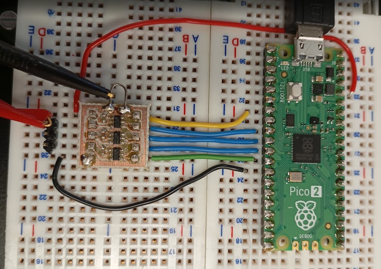
I’m using the RP2350W, so far only in 6-step mode, which worked fine. Now I want to move to FOC. I designed a board rated 600 VDC with full isolation between Pico 2 and HV side. It has zero-crossing comparators, isolated current and bus-voltage sensing, plus braking. You’re welcome to copy it: https://carnetic.com/wp-content/uploads/2025/09/BLDC-Direct-by-RPI-Pico-fully-isolated.zip And if you know how to implement SimpleFOC, pls. reply.
– skolnes