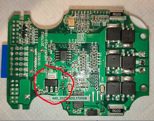
I’m going through the IHSV57 PCB and I’ve found a spot which is a bit unclear to me. Maybe someone has an idea what this part should be about. I think it’s some kind of filter - but for what?
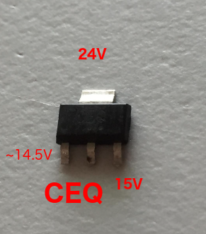
The central component there is labelled as “CEQ” it seems to output 15V on one pin and around 14.5V on the other one. Does anyone have an idea what that should be?
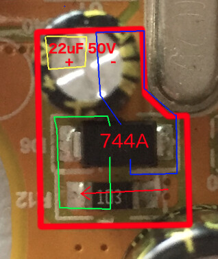
I took the green PCB screenshot from a JMC teardown from this forum, my PCB is a bit newer and the encoder has changed it seems.
I don’t think this circuit is for burning the generated power which comes back from the motor during deceleration.
Also I wonder what this SOT223 is (which outputs 15v on one pin, and 14.xx on the other one) for I couldn’t find anything about it neither did I ever work with an IC like that before.
That looks like a 24v to 15v LDO to support probably the mosfet gate drivers? I suppose your board has 24v powered MOSfets which need to be driven by about 15v gates.
Yeah that’s probably the reference line, hard to tell without a part number. I’m more curious why they connected with with a 0O resistor to the high power rail, lol, and no buffer capacitance. Unless there are components on the back, I see a bunch of through holes manually soldered components there, may be I’m overthinking here and being unfair to the original designer.
It would be helpful if we had high quality photos of both sides. Reverse engineering this would not even require an x-ray if it’s just a dual layer, only a pen and paper and a microscope and a cup of coffee. Beats a sudoku any day of the week.
My first assumption that this is a 2 layer board was wrong - my current assumption is it’s a 4 layer board.
It’s an LDO which is connected to the pre-drivers. I only put the pre-driver into my schematic and did not finish the VCC circuit (I’m still working on reverse engineering the entire board)
I want a modified version of this motor driver which can also return an index pulse which I can use as a second stage for accurate homing.
The board I’m working on has a burned STM32F1 (seems like they changed it to a Nation ARM Cortex-M4 later) I plan to put an STM32F4 in and start playing with it after reconstructing the entire pinout.
You’ll need to x-ray the board, and at different angles to catch overlapping traces. 4-layer is still possible to x-ray, more than that it’s a destructive effort, where you need to remove the components, dump it in a tin bath to clean it and then dissolve in solvent and peel off the layers.
Cheers,
Valentine
PS this is extremely dangerous and requires professional PPE, specialized equipment and access to industrial solvents, you cannot do it in a DIY environment.
I feel like the circuit is easy, no need to X-ray this one.
Right now I just need to finalize the sensor part, afterwards I’ll put my STM32F4 on it and use it as playground for further BLDC development. I think this is a pretty good playground.