Found these tiny active balancing IC´s ETA3000. They will only balance to cell´s next to each other, so for a 14 cell battery it is not suitable, unless you are able to use it within a switch matrix. It is very suitable for a 3 cell battery, and can run more ore less autonomously. This could be the solution for balancing the balance battery… It can go up to 2 amps according to the datasheet, but that would be pushing it and is more then needed.
What’s the overall strategy? What circuitry do you have per-cell, and what is central?
I guess the 14 cells have to stay connected in each parallel pack, to maintain the target voltage. But you could disconnect one set of 14 from the output and balance charge its cells while the remaining cells act as a 14S3P pack? Or how does that work?
I think im getting closer to a strategy. The 14S4P battery will have each cell connected to a bus, through a switch matric. The way TI demonstrates using the EMB1499Q for a 14 cell battery, is to have two EMB1428 (7 cell switch matrix) mowing current from top 7 cells to bottom 7 cell´s or opposite. Somewhere I found a illustration, where they have a battery in between. This approach uses a lot of components (two transformers included + MCU).
I believe the best strategy is to have the MCU do the switch matric of the entire pack. So one cell can charge or discharge current through a single transformer to the 3 cell battery. The 3 cell battery will more or less act as a buffer, like all batteries do more or less.
Under all circumstances we need the 11.1 (12v) for switching the mosfet´s inside the BLDC controller and the ones in the battery pack. Doing it this way combines the voltage stepdown for the BLDC controller and the battery balancing. If the 3 cell battery runs low, then the balancing will start to draw current from the 14S4P cell with the highest voltage (semi active balancing). To move charge from a cell with high voltage to a low one, it has to go through the 3 cell battery.
To put things in perspective; the EMB1428 is 21$ in low quantities. A NPN/PNP transistor is way less. The dedicated switch matrix may have some clever safety features, but for a small 14S4P, in comparison to larger batteries, it is to costly. The switches is going to be on/off, so no consideration for switching losses needed. In larger quantities NPN/PNP transistors are just a fraction of a $ and because we have to integrate a MCU no matter what, I believe this is the way forward. There may be some space considerations for using the EMB1428, but surely they do not apply here.
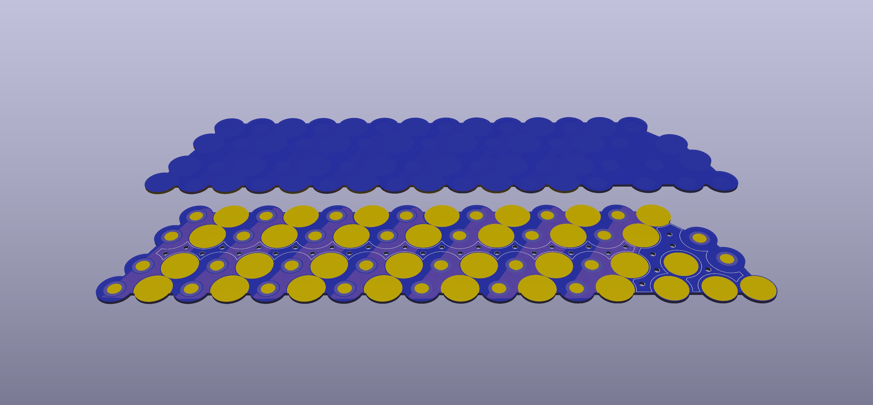
Just made a JLCPCB test “quote” for a 380mm x 100mm PCB. Came out to around 20$ for five psc plus 35$ engineering fee. That´s actually within reason.
Regarding the safety concerns. Having 1.6mm FR4 PCB on either side of the batteries will obviously be safer then a shrink wrap.
There may be a way to combine the spot welding approach with the integrated PCB balancer. Let´s say you pre-spot welded the cell´s (4 x 2170 cell´s). With the nickel strip on there, it should be easy to make a good solder connection to the board. That would bind the whole think together, but changing batteries might be a hassle.
")
Have been thinking further about this balancing act; Trying to simplify and cut the cost.
Maybe the isolated dc-dc is overkill, even though it does sound nice.
Idea: What if the switch matric (controlled by the MCU), capable of isolating single cell´s out, in order to balance the cell´s, was expanded to each side of the High Voltage Pack and the Low voltage Pack. Like a side-by-side or bidirectional dc-dc converter (without the isolation). This way, the current will flow from one cell in the HV-Pack to a single cell in the LV-pack, thereby balancing both sides in the process.
When charging the HV-pack, the LV-pack will charge trough balancing, and is capable of moving power to a low voltage cell.
Not sure the isolation is required.
Using a dedicated 14cell monitor and balancer to control the gates of the balancing bus (through SPI or I2C). These IC´s has some really good implementation of cell voltage, temperature, SOC monitoring and so on, plus the ones made for passive balancing is capable of driving the balancing-bus-FET´s just as well as a MCU. This free´s up lots of IO pins, so a small MCU can be used in a modular break-out board fashion, with the dc-dc step-down/step-up on-board. This approach will make it possible to have several different implementations for the controller and dc-dc circuit.
Will try to do a mockup with the needed breakout pins.
Note to self: remember a fuse.
Further reducing BOM by using MCU controlled boost dc-dc converter could be the end goal here. I already have some experience with the SAME51 and do have some stock for experimentation. This MCU has lots of IO pins and it has the hardware to do SMPS boost converter. Using the already existing timer and switching firmware in SimpleFoc hardware specific, could be useful for implementing a boost charging algorithm/control loop for moving charge between two cell’s. The CAN FD functionality in this MCU gives it a advantage for communicating with the motor controller, which is the basic idea of this concept, in order to synchronize the energy storage and energy consumption (battery and motor control relation, especially with regards to safety aspects of over-discharge and so on) by having the BMS talk to the motor controller.
Someone already had this idea: Control Half Bridge/Full bridge for Synchronous Buck/Boost? · Issue #132 · simplefoc/Arduino-FOC · GitHub
You could drop them a line and see if they made any code for it?
Nice, but totally different voltage level. He is messing with 380v ![]() Luckely the battery cell (3.7v) low voltage will allow the use of ultra low Rds(on) switches. I’m thinking not to overthink it. Basically it is straight forward. Will find a reference design in order to match the CAP and inductor values. Since the MCU will know the cell voltage, it should be possible to do basic CC constant-current and constant voltage.
Luckely the battery cell (3.7v) low voltage will allow the use of ultra low Rds(on) switches. I’m thinking not to overthink it. Basically it is straight forward. Will find a reference design in order to match the CAP and inductor values. Since the MCU will know the cell voltage, it should be possible to do basic CC constant-current and constant voltage.


Mkay, some progress on the concept
I am digging through the BQ75614 datasheet and think it is a good candidate in combination with the SAME51 MCU.
TI uses a isolated Uart level shifter, which brings up a lot of issues to consider. Isolated vs. common-gnd. First of all, the isolation IC uses 1.2mA when disabled, and since there should always be some means to wake the BQ75614, 1.2mA is a conservative estimate. This means the system has a hard time to go into SHUTDOWN mode, and would drain the pack over time (more then necessary)
Another downside to galvanic isolation, is the fact that we cant switch the MOSFET´s without isolated gate drivers as well, which means higher cost again.
If on the other hand, the HV pack and the LV pack share a common ground, but uses different channels/wires to source, the two packs will not see each others current draw and would in my opinion dampen the motor transient noise?
Do you see any issues with relation to having a 14 sell pack share GND with a 3 sell pack ?
The BQ75614 has separate sense and balance pins for each sell, which means it can use 10ohm resistors for balancing.
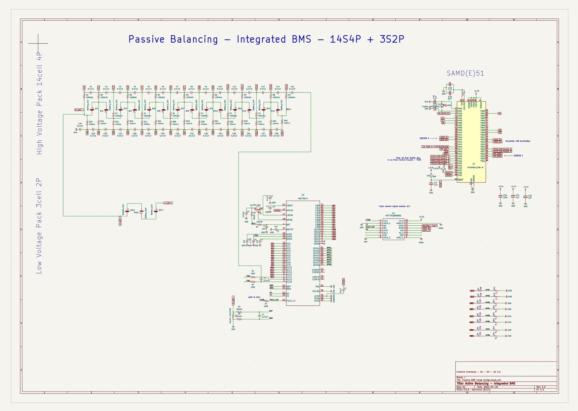
Edit: The cool thing about BQ75614 is, that it is pin compatible with other TI balancing ICs which can be stacked. Those do require some additional circuitry for linking the stacks, but the option is there. Maybe it makes more sense to use the CAN bus
")
Ok,
Ive come to the conclusion, while considering a bidirectional DC/DC converter-solution, that a dedicated charge BUCK converter is the optimal approach for charging the secondary 3S2P battery. The MCU does not have PWM resolution to drive a BUCK converter at high frequency. It is possible to have the SAME51 do the switching, but the inductor value will have to be accordingly high and therefore large. Likewise the capacitors need considerable higher capacity.
Using the MAX17703 (60v to 12.6v) at a 1650khz freq. the inductor can be kept to 10uH. This charge IC has some clever safety features, like thermistor temp programming to suspend charge below/above eg. +5 to +45 Celsius. It has a pre-charge voltage setting, which will charge the battery at just 1/10 the MAX current until the CC (Constant Current) level is reached.
When the main (14 cell) pack is charging, the MAX17703 will draw current from the incoming charge current. Depending on temperature and other settings, the charge current can be set to low (60%) or high (50mV on shunt resistor).
Power_dissipation can be calculated using this TI BUCK_CALC sheet
